
Prof. Dr. Thorsten Jungmann (last updated 2026-10-13)
Relates to DET-02 Logic operations
Task
Logic gates make decisions everywhere: in your smartphone, in machines and in the controller of a heat pump. Engineers describe a gate in whichever of seven forms of representation suits the task at hand. In this exercise, you describe each of the seven gates of the lesson in two of these forms, so that you practise each form twice.
All gates except the NOT gate have the two inputs and ; the NOT gate has only the input . The output is always . Draw schematic symbols according to the standard of the International Electrotechnical Commission (IEC), IEC 60617, and contact logic between the rails L+ and L−. In timing diagrams, the inputs run through all their combinations one after another, in the order of the truth table and each for the same time; assume ideal gates without delay. Give VHDL code as the signal assignment of the output.
a) Draw the contact logic of the NOT gate and sketch its timing diagram.
b) Draw the Karnaugh map of the AND gate and give its VHDL code.
c) Set up the truth table of the OR gate and sketch its timing diagram.
d) Give the logic expression of the NAND gate and draw its contact logic.
e) Draw the schematic symbol of the NOR gate and give its VHDL code.
f) Give the logic expression of the XOR gate and draw its Karnaugh map.
g) Set up the truth table of the XNOR gate and draw its schematic symbol.
Solution
Given
Given explicitly:
- the seven gates NOT, AND, OR, NAND, NOR, XOR and XNOR with the inputs and , the NOT gate with the input only, and the output
- a) to g) two forms of representation for each gate
- timing diagrams: all combinations of the inputs in the order of the truth table, each for the same time; ideal gates without delay
- VHDL code: the signal assignment of the output
Known:
- The seven forms of representation and their purposes (DET-02), each form in detail in DET-02 to DET-02
- The seven gates (DET-02 to DET-02); the qualifying symbols according to the standard of the International Electrotechnical Commission (IEC), IEC 60617 (DET-02)
Required
a) the contact logic and the timing diagram of the NOT gate
b) the Karnaugh map and the VHDL code of the AND gate
c) the truth table and the timing diagram of the OR gate
d) the logic expression and the contact logic of the NAND gate
e) the schematic symbol and the VHDL code of the NOR gate
f) the logic expression and the Karnaugh map of the XOR gate
g) the truth table and the schematic symbol of the XNOR gate
a) NOT gate: contact logic and timing diagram
The NOT gate, the inverter, delivers the opposite of its input (DET-02, 3.1):
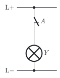
In contact logic, a normally closed contact stands for the negation of its variable (DET-02, 2.5). The inverter is therefore a single normally closed contact in series with the lamp . As long as nobody actuates the contact, , it is closed and the lamp lights; when it is actuated, , it opens, and the lamp goes out:
In the timing diagram, the input runs through its two values, first 0 and then 1 (DET-02, 2.7). The output is the mirror image of the input:
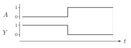
Check with the truth table of the inverter: and . The lamp lights in the first section, while the contact is not actuated, and goes out in the second ✓
b) AND gate: Karnaugh map and VHDL code
The AND gate delivers a 1 only if both inputs are 1 (DET-02, 3.2):
The Karnaugh map arranges the truth table as a grid, with two rows for and two columns for (DET-02, 2.6). Of the four cells, only the cell for and contains a 1:
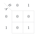
In VHDL, the operator and stands for the AND operation (DET-02, 2.8). The signal assignment of the output is:
Y <= A and B;Check: the cell with the 1 belongs to row 3 of the truth table, the only row in which both inputs are 1 ✓
c) OR gate: truth table and timing diagram
The OR gate delivers a 1 if at least one input is 1 (DET-02, 3.3):
With two inputs, the truth table has rows, in ascending order like a binary count and numbered from row 0 to row 3 (DET-02, 2.2):
| 0 | 0 | 0 |
| 0 | 1 | 1 |
| 1 | 0 | 1 |
| 1 | 1 | 1 |
In the timing diagram, the inputs run through the four rows of the truth table one after another, each for the same time; section by section, the output follows the column (DET-02, 2.7):
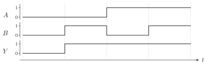
is 0 in the first section and rises to 1 as soon as becomes 1 at the start of the second section.
Check with the rule of the OR gate: is 0 only in row 0, where neither input is 1, and so only in the first section of the timing diagram ✓
d) NAND gate: logic expression and contact logic
The NAND gate is an AND gate with an inverted output: its output is 0 only if both inputs are 1 (DET-02, 4.1). Its logic expression is:
The bar covers the whole product: first and are combined, then the result is negated. Careful: ; the right-hand side is the NOR operation.
For the contact logic, De Morgan’s law helps (DET-02, 5.5): , the OR of the two negated inputs. A normally closed contact stands for a negated input (DET-02, 2.5), and contacts in parallel stand for OR (DET-02, 3.3). So two normally closed contacts lie in parallel, in series with the lamp :
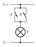
The lamp goes out only if both contacts are actuated and both open.
Check for and : both normally closed contacts are open, so the lamp is out, and the expression gives . In each of the other three combinations, at least one contact stays closed, and the lamp lights, ✓
e) NOR gate: schematic symbol and VHDL code
The NOR gate is an OR gate with an inverted output: its output is 1 only if both inputs are 0 (DET-02, 4.2):
Its schematic symbol according to IEC 60617 is the OR symbol, a rectangle with the qualifying symbol ≥1, with a negation circle at the output (DET-02, 2.4, DET-02, 4.5):
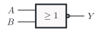
In VHDL, the operator is nor (DET-02, 2.8):
Y <= A nor B;Check with the rule of the qualifying symbol: ≥1 delivers a 1 if at least one input is 1, and the negation circle turns this into a 0. So is 1 only if both inputs are 0, as the expression says ✓
f) XOR gate: logic expression and Karnaugh map
The XOR gate delivers a 1 if its two inputs are different (DET-02, 4.3). Its logic expression, written once with the XOR operator and once with AND, OR and NOT, is:
Read: ‘Y equals A exclusive-or B’. The right-hand side says the same: either is 0 and is 1, or is 1 and is 0.
In the Karnaugh map, the two 1s therefore lie in the cells for , and for , , diagonally opposite each other (DET-02, 2.6):
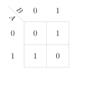
Check: in the truth table of the XOR gate, is 1 in rows 1 and 2; these are the cells for , and for , . Each of the two products of the expression stands for one of these cells ✓
g) XNOR gate: truth table and schematic symbol
The XNOR gate is an XOR gate with an inverted output: it delivers a 1 if its two inputs are equal, which is why the operation is also called equivalence (DET-02, 4.4):
The truth table has rows (DET-02, 2.2):
| 0 | 0 | 1 |
| 0 | 1 | 0 |
| 1 | 0 | 0 |
| 1 | 1 | 1 |
Its schematic symbol according to IEC 60617 is the XOR symbol, a rectangle with the qualifying symbol =1, with a negation circle at the output (DET-02, 4.4, DET-02, 4.5):
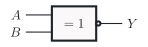
The standard also has a symbol of its own for the equivalence, with the qualifying symbol =, which you will find in German textbooks.
Check: is 1 in rows 0 and 3, where and are equal, and 0 in rows 1 and 2, where they differ: exactly the opposite of the XOR gate in f) ✓