In the previous lesson, you got to know the organization of this module and took a first look at digital electronics.
Analogue signals map information continuously; digital signals encode it with the two values 0 and 1, each of which is assigned to a range of the voltage.
The bit is the smallest unit of information. In positive logic, HIGH stands for 1 and LOW for 0.
In a positional number system, each digit is weighted with a power of the base. You converted numbers between the decimal, binary, octal and hexadecimal systems.
You added and subtracted binary numbers and represented negative numbers in two’s complement.
Today, we look at the circuits that process these bits: how they are built and how they combine bits with one another.
1 Switches made of silicon – From the transistor to the CMOS circuit
1.1 Processors, gates and transistors
In the previous lesson, the bit was our leading character: a voltage that lies either in a lower or in an upper range. Today, we ask what produces these voltages and combines them with one another.
The processor of your smartphone and the microcontroller on the control board of the heat pump are integrated circuits (IC, German: integrierte Schaltungen): all their components are made together on a single chip of semiconductor [5, p. 62], and they consist of logic gates. A logic gate (German: Logikgatter) is a circuit that carries out one of the basic operations of the binary system, such as inverting a bit or combining two bits [5, p. 43]. Each gate consists of a few transistors. A transistor (German: Transistor) is a component made of a semiconductor that works as an electrically controlled switch in a digital circuit. Modern integrated circuits contain billions of them [5, p. 62].
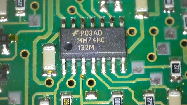
The photo shows an integrated circuit from the 74HC family that contains four logic gates. There are two kinds of transistors. The bipolar junction transistor (BJT, German: Bipolartransistor) is controlled by a current: a small current into its base switches a larger current between its two other terminals, and the base current has to keep flowing to keep it on [5, p. 71]. The classic transistor–transistor logic (TTL) from DET-01 is built from bipolar transistors. The metal oxide semiconductor field-effect transistor (MOSFET, German: MOS-Feldeffekttransistor) is controlled by a voltage: an electric field at its insulated gate switches it on or off [5, p. 62].
Digital electronics today uses almost only MOSFETs, for three reasons:
Control without power: The gate of a MOSFET is insulated. Once it is charged, holding the switch on or off needs practically no power.
No current at rest: In complementary metal oxide semiconductor (CMOS) technology, two kinds of MOSFET work in opposite ways, so that no current flows from the supply to ground as long as nothing switches [5, p. 64]. A TTL gate, in contrast, draws current through a resistor whenever its output is LOW [5, p. 72].
Small size: MOSFETs can be made tiny and packed densely; TTL cannot reach the density that today’s processors need [5, p. 71].
Bipolar transistors are still found in analogue amplifiers, but not in the billions of switches of a processor. The MOSFET, however, is not an ideal switch either: when it is on, it has a small resistance, and its gate has to be charged first. Section 3.5 shows the consequence: every logic gate needs a little time.
1.2 Inside the MOSFET
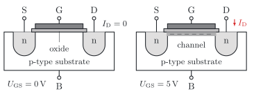
Why the MOSFET is such a good switch becomes clear from its structure (figure). Its name lists the layers under its control terminal: a metal electrode, a thin insulating oxide layer and the semiconductor below – metal oxide semiconductor. Field effect names the principle: an electric field, not a current, controls the transistor.
A MOSFET has four terminals: the gate (G), which controls it, the source (S) and the drain (D), between which the current flows, and the bulk (B), the connection of the substrate, which lies at a constant potential in CMOS circuits [12, p. 39]. Do not confuse the gate of a transistor with a logic gate: both take their name from the gate in a fence, which lets something pass or not – the gate of the transistor opens and closes the channel, the logic gate lets a signal through or blocks it.
In an n-channel MOSFET, source and drain are two n-doped regions in a p-doped substrate (German: Substrat). Without a voltage at the gate, no current flows between them, because the p-doped silicon in between offers no conducting path from one n region to the other. If the gate is made positive with respect to the source, by more than the threshold voltage (German: Schwellenspannung) Uth, its electric field draws electrons to the surface under the oxide. They form a thin conducting channel (German: Kanal) between source and drain, and a current can flow [5, p. 63]. The oxide insulates the gate, so that no current flows into it: once the gate is charged, holding the transistor on or off needs practically no power [12, p. 39].
This type is the n-channel MOSFET (NMOS, German: n-Kanal-MOSFET). The p-channel MOSFET (PMOS, German: p-Kanal-MOSFET) is built the other way round, with p-doped regions in an n-doped substrate, and conducts when its gate is lower than its source by more than the threshold voltage [5, p. 63]. Why doping creates n- and p-type regions goes beyond this module; the page on semiconductors gives a first impression.
1.3 The MOSFET as a switch
As a switch, a MOSFET knows two states [5, p. 63]. An NMOS switches on when the voltage between gate and source, UGS, is greater than its threshold voltage Uth, typically 0.2 V to 1 V; then its channel connects source and drain. A PMOS switches on when its gate is lower than its source by more than the threshold voltage. Put simply, for a digital circuit this means: an NMOS closes when there is a 1 at its gate, and a PMOS closes when there is a 0 at its gate.
Complementary metal oxide semiconductor (CMOS) technology combines both types in every logic gate. Complementary means that the two complete each other: one type switches on exactly when the other switches off [5, p. 62].
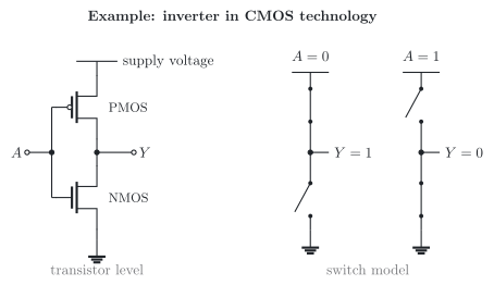
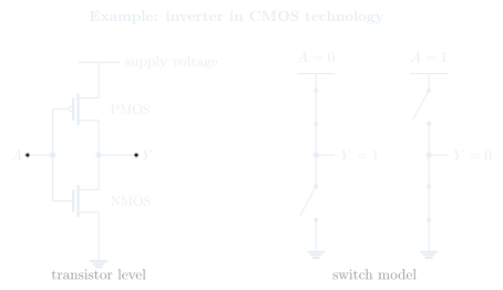
The simplest CMOS circuit has two transistors (figure). A PMOS connects the output Y to the supply voltage, an NMOS connects it to ground; the gates of both are connected to the input A. If A=0, the PMOS is on and the NMOS is off: the output is connected to the supply voltage, and Y=1. If A=1, it is the other way round: the output is connected to ground, and Y=0 [5, p. 64]. Because the output is always the opposite of the input, the circuit is called an inverter (German: Inverter) [5, p. 64].
Since one of the two transistors is always off, no current flows from the supply to ground in either state. Current flows only for a short time while the output switches, because the inputs connected to it have to be charged or discharged [12, p. 50]. This is why CMOS circuits need so little power – and why DET-01 could promise that a digital circuit that inverts a signal needs only two transistors. Section 3.1 of this lesson introduces this circuit as the NOT gate, the first of the basic gates.
2 One operation, seven views – Forms of representation of logic circuits
2.1 Seven ways of describing a gate
In chapter 1, you met the inverter as a circuit of two transistors. Engineers, however, describe a logic circuit in whichever form suits the task at hand: one form is best for designing, another for analysing, simulating or documenting it. In this module, we use seven forms of representation (German: Darstellungsformen), among them code in the very high speed integrated circuit hardware description language (VHDL). Each form serves its own purpose:
In this chapter, we go through the seven forms with the AND gate as our example. Unlike the inverter, it has at least two inputs, and only then does every form show what it can do. The example comes from your smartphone. During a call, the display switches off as soon as you hold the phone to your ear: a proximity sensor next to the earpiece detects that something is covering it. Your cheek cannot press any buttons by mistake, and the display does not waste energy.
The display goes dark only if both conditions are met: a call is active, and the sensor is covered. The sensor alone is not enough – otherwise the display would go dark whenever your hand passes over the top of the phone. The call alone is not enough either, because you want to see the display when you are talking over the loudspeaker. We name the two inputs and the output:
A: a call is active
B: the proximity sensor is covered
Y: the display is off
The ‘and’ of everyday language is the AND operation. In the following sections, we describe it in all seven forms; section 3.2 then sums it up as a basic gate.
2.2 Truth table
The truth table (German: Wahrheitstabelle) defines a logic function completely: it lists every possible combination of the inputs and, for each of them, the value of the output [5, p. 44]. With n inputs, there are 2n combinations, as you know from DET-01, 5.3. The combinations are always listed in ascending order, like a binary count from 0, so that each row number is the decimal value of the input code [5, p. 44]. The leftmost input has the highest weight. For our example:
A
B
Y
0
0
0
0
1
0
1
0
0
1
1
1
Only in the last row, call active and sensor covered, is the display off. A circuit with several outputs has one column per output. The table is complete and easy to check row by row; with every additional input, however, it doubles in length.
2.3 Logic expression
The logic expression (German: Ausdruck) describes the output as an equation of the inputs [5, p. 44]. For the AND operation, the operator is the dot, because the operation behaves like a multiplication of 0 and 1: the product is 1 only if every factor is 1 [5, p. 46]. This is why it is also called the logical product:
Y=A⋅B
where:
Y is the output, here ‘display off’, 0 or 1
A is the first input, here ‘call active’, 0 or 1
B is the second input, here ‘sensor covered’, 0 or 1
Read: ‘Y equals A and B’. The dot may be omitted, as in Y=AB. A circuit has one expression for each output [5, p. 44].
The dot for AND, the plus sign for OR and the bar for NOT form the notation of electrical engineering, which we use in this module. Mathematics and computer science use other notations for the same operations; chapter 5 sets them side by side.
Compared with the truth table, the expression stays short and can be transformed with the rules of Boolean algebra; however, you have to evaluate it to see the output for a particular combination.
2.4 Schematic symbol
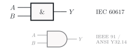
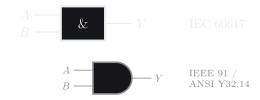
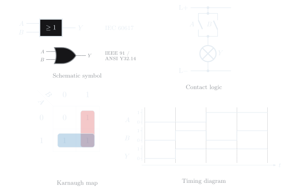
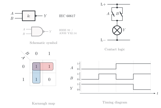
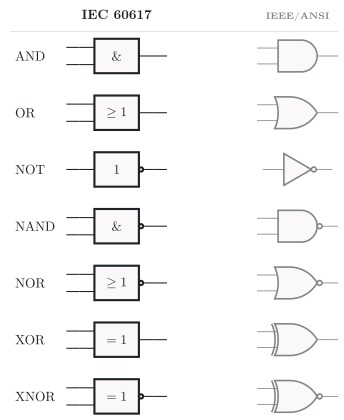
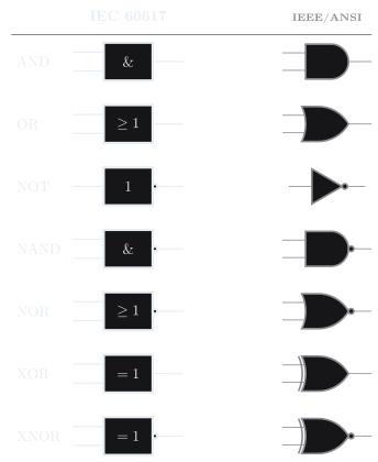
The schematic symbol (German: Schaltzeichen) represents a gate in a schematic. Two sets of symbols are in use (figure). The International Electrotechnical Commission (IEC) draws every gate in its standard IEC 60617 as a rectangle with the inputs on the left and the output on the right; a qualifying symbol (German: Kennzeichen) inside states the function, for the AND gate the ampersand & [12, p. 17]. American textbooks such as LaMeres [5] and many datasheets use the distinctive shapes that the Institute of Electrical and Electronics Engineers (IEEE) and the American National Standards Institute (ANSI) laid down in IEEE 91 / ANSI Y32.14; in them, the AND gate looks like a capital D. In this module, we draw all circuits according to IEC 60617. In this lesson, however, every gate appears in both sets, so that you can read both; the American symbol is grey and a little smaller.
2.5 Contact logic
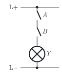
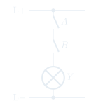
Contact logic (German: Kontaktlogik) is the electrical counterpart of a gate: the inputs are switches or relay contacts, and the output is a load such as a lamp between the two rails L+ and L−. An actuated contact stands for a 1 at the input, a lit lamp for a 1 at the output. A normally open contact (German: Schließer) closes when it is actuated and therefore stands for the variable itself. A normally closed contact (German: Öffner) opens when it is actuated and therefore stands for the inverted variable. For the AND gate, two normally open contacts lie in series: the lamp lights only if A and B are both actuated.
Contact logic is more than a teaching aid. In control cabinets, relays and contactors carried out logic long before there were transistors, and the control board of our heat pump still switches pumps and valves via relays (DET-01, 3.4).
From relay contacts to Boolean algebra
In his master’s thesis of 1937, Shannon showed that circuits made of relay contacts can be described and minimized with Boolean algebra. This idea became the foundation of digital circuit design.
2.6 Karnaugh map
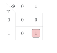
The Karnaugh map (German: KV-Diagramm) arranges the truth table as a grid: each cell stands for one combination of the inputs and contains the output for it. For two inputs, the grid has two rows for A and two columns for B (figure). The AND gate has a single 1, in the cell for A=1 and B=1. The map is named after Karnaugh, who refined it in 1953 from a chart by Veitch; in German, it is therefore also called the Karnaugh-Veitch-Diagramm. It makes sense only with two or more inputs. Its strength shows when expressions are to be minimized: neighbouring cells reveal which inputs have no influence on the output. We use it for this in DET-03.
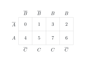
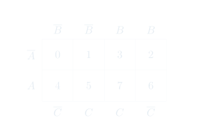
With three inputs, the grid has two rows and four columns (figure). The labels at its edges show where each input is 1: A on the left, B above and C below the grid, in a row of its own. A plain letter marks the row or the columns in which the input is 1, a letter with a bar those in which it is 0. Read from left to right, the columns stand for BC = 00, 01, 11, 10: from one column to the next, only one input changes, and this also holds between the last column and the first [5, pp. 126–127]. Each cell takes the output of one row of the truth table, 0 or 1; in the figure, it shows the number of this row instead. Rows 2 and 3 therefore swap places, and so do rows 6 and 7. To fill in the map, you go through the truth table row by row and enter each output in the cell with the number of its row.
2.7 Timing diagram
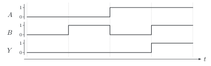
The timing diagram (German: Zeitdiagramm) shows the signals over time [5, p. 45]. Each signal is either 0 or 1, so that it jumps between two levels. In our timing diagrams of gates, the inputs run through all combinations one after another, in the order of the truth table and each for the same time interval; the output below them shows the result. The output of the AND gate is 1 only in the last interval. A timing diagram resembles what you would see when measuring a real circuit with an oscilloscope [5, p. 45] or a logic analyser. It is the only one of the seven forms that shows time, and so it reveals what the others hide: in which order signals change.
Our timing diagrams of gates are ideal: the output changes at the same moment as the inputs. Real gates need a little time for this. Section 3.5 shows how much, and chapter 6 shows how the delays of several gates add up in a circuit.
2.8 VHDL – circuits described as text
Schematics work well for a few gates. For larger designs, however, they soon became too cumbersome, and descriptions in words became too long to be useful. In 1983, the American Department of Defense therefore started a programme for a language that describes the behaviour of digital circuits as text. The result was VHDL, released in 1985 and standardized by the IEEE in 1987 [5, p. 156].
VHDL is a hardware description language (German: Hardwarebeschreibungssprache): its code looks like a program, but it describes hardware. Tools simulate the description and turn it into a circuit, for example on a programmable logic device, which you will meet in DET-10. Besides VHDL, Verilog is the other widely used hardware description language [5, p. 155].
A design in VHDL has two parts [5, p. 165]. The entity describes the interface: the inputs and outputs, called ports (German: Anschlüsse), each with its name, its direction in or out and its type, here bit with the values 0 and 1 [5, pp. 166, 168]. The architecture describes the behaviour [5, p. 169]. For the display of our smartphone, the design looks like this:
-- A: call active-- B: proximity sensor covered-- Y: display offentity display_off is port (A, B : in bit; Y : out bit);end entity;architecture behaviour of display_off isbegin Y <= A and B;end architecture;
The line with <= is a signal assignment (German: Signalzuweisung): the output Y receives the result of A and B [5, p. 171]. Two dashes start a comment, and a semicolon ends each statement. Unlike the lines of a program, the assignments of an architecture are not executed one after another. Each of them is a piece of hardware, and all of them work at the same time; they are concurrent (German: nebenläufig) [5, p. 171].
For each gate, VHDL has its own logical operator [5, p. 172]:
Operator
Operation
Example
not
NOT
Y <= not A;
and
AND
Y <= A and B;
or
OR
Y <= A or B;
nand
NAND
Y <= A nand B;
nor
NOR
Y <= A nor B;
xor
XOR
Y <= A xor B;
xnor
XNOR
Y <= A xnor B;
The inverter from chapter 1 differs from the display only in its name, its ports and its assignment:
entity not_gate is port (A : in bit; Y : out bit);end entity;architecture behaviour of not_gate isbegin Y <= not A;end architecture;
Your aim is to recognize VHDL code of a logic operation and to sketch the corresponding circuit; chapter 6 practises this with a larger example.
3 All or one – Basic gates
3.1 The NOT gate
Seen from outside, the circuit of section 1.3 does something very simple: its output is always the opposite of its input. This logic operation is the negation (German: Negation), also called the NOT operation, and the gate that carries it out is the NOT gate, also called the inverter [5, p. 46]. It is the first of our basic gates.
Its truth table has only two rows, one for each value of the input:
A
Y
0
1
1
0
As an equation, the negation is written with a bar over the variable:
Y=A
where:
Y is the output of the inverter, 0 or 1
A is the input of the inverter, 0 or 1
Read: ‘Y equals not A’ or ‘Y equals A bar’. LaMeres also writes A′ [5, p. 46]; in this module, we use the bar.
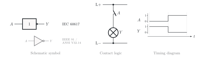
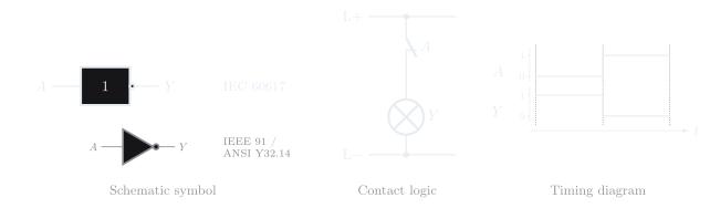
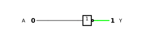
The figure shows three further forms. The schematic symbol according to the standard of the International Electrotechnical Commission (IEC), IEC 60617, is a rectangle with the qualifying symbol 1; the small circle at the output, the negation circle (German: Negationskreis), stands for the negation. The American symbol is a triangle with a small circle. In contact logic, the inverter is a normally closed contact: as long as nobody actuates it, it is closed and the lamp lights; when it is actuated, A=1, it opens, and the lamp goes out. The timing diagram shows the output as the mirror image of the input. In VHDL, the inverter is the operator not (section 2.8).
You use a negation every day. Your smartphone rings audibly only if it is not switched to silent: with A for ‘silent mode on’ and Y for ‘ringtone audible’, Y=A – leaving aside the other settings of the phone. Many heat pumps have an input for a blocking signal of the energy supplier: as long as it is 1, the heat pump must not start [13]. The release for the compressor is therefore, put simply, the negation of this signal.
In the simulator, you can switch the input and watch the output follow as its opposite.
3.2 The AND gate
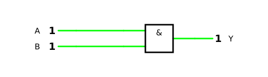
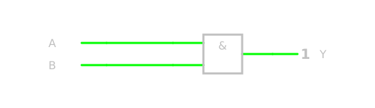
Chapter 2 used the AND operation as its example; now we can state it formally: the AND gate (German: UND-Gatter) delivers a 1 at its output only if all its inputs are 1 [5, p. 46]. After the NOT gate, it is the second of our basic gates. In chapter 2, you have seen it in all seven forms:
the truth table with a single 1 in the last row and the expression Y=A⋅B (sections 2.2 and 2.3),
the schematic symbol with & and two normally open contacts in series (sections 2.4 and 2.5),
the Karnaugh map with a single 1 and the timing diagram in which the output is 1 only in the last interval (sections 2.6 and 2.7),
the VHDL operator and (section 2.8).
The AND gate is the gate of conditions that all have to be met. In the smartphone, the display goes dark only during a call and with the sensor covered. A heat pump could, for example, start its compressor only if there is a demand for heat and the energy supplier allows it to run – the release that we formed in section 3.1 as the negation of the blocking signal. And in a machine, a press may only move down if the guard is closed and both hands of the worker are on the two buttons.
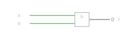
In the simulator, you can switch both inputs and watch the output: it shows a 1 only when both inputs are 1. Try all four combinations and compare them with the truth table.
An AND gate is not limited to two inputs: for the press, a single AND gate with three inputs checks all three conditions at once. Section 3.4 shows more about gates with many inputs.
3.3 The OR gate
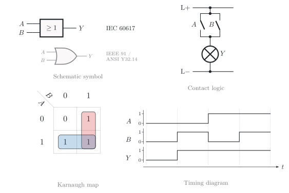
The third basic operation is the OR operation. The OR gate (German: ODER-Gatter) delivers a 1 if at least one of its inputs is 1 [5, p. 47]. Your smartphone shows it every time you pick it up: the screen switches on if you press the power button or if you lift the phone. Either is enough, and both together do no harm. With
A: the power button is pressed
B: the phone is lifted
Y: the screen is on
the truth table and the expression are:
A
B
Y
0
0
0
0
1
1
1
0
1
1
1
1
Y=A+B
where:
Y is the output, here ‘screen on’, 0 or 1
A is the first input, here ‘power button pressed’, 0 or 1
B is the second input, here ‘phone lifted’, 0 or 1
Read: ‘Y equals A or B’. The plus sign stands for the logical sum [5, p. 47]. Careful: in Boolean algebra, 1+1=1. All that matters is whether at least one input is 1, not how many. The 1+1=102 of DET-01 belongs to the addition of binary numbers, which is a different operation.
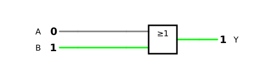
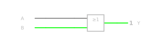
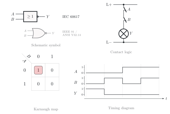
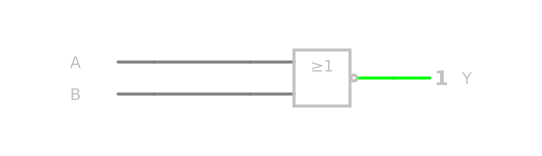
The figure shows the other forms. The qualifying symbol ≥1 in the rectangle states the rule: at least one input is 1. In contact logic, the normally open contacts lie in parallel, so that either of them can light the lamp. The Karnaugh map contains a 0 only in the cell for A=0 and B=0, and in the timing diagram, the output is 0 only in the first interval. In VHDL, the OR operation is the operator or:
In the simulator, the output already shows a 1 when a single input is 1. Where the AND gate checks that all conditions are met, the OR gate checks whether at least one of them is met.
3.4 Gates with more than two inputs
AND and OR gates are not limited to two inputs [5, pp. 46–47]. An AND gate with n inputs delivers a 1 only if all n inputs are 1; an OR gate with n inputs delivers a 1 if at least one of them is 1. The truth table grows to 2n rows, the rectangle of the schematic symbol simply gets more input lines, and in contact logic, more contacts lie in series or in parallel.
This answers our first guiding question. A car has four doors and a boot, and each of them has a door contact that delivers a 1 when it is open. The interior light is to switch on as soon as any one of them is open – an OR with five inputs:
Y=A+B+C+D+E
where:
Y is the output, here ‘interior light on’, 0 or 1
A to D are the inputs ‘door 1 open’ to ‘door 4 open’, each 0 or 1
E is the input ‘boot open’, 0 or 1
In contact logic, these are five normally open contacts in parallel: whichever door is opened, it closes a path to the lamp.
Image by Qwen-Image 2.1
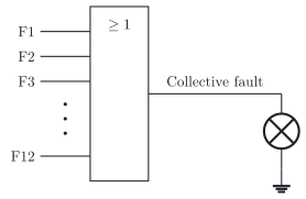
The same idea makes a single warning lamp light up as soon as any one of a dozen faults occurs, our second guiding question. The controller of our heat pump reports its state in individual status bits, and among them is a bit for the collective fault (German: Sammelstörung). Such a bit can be formed as the OR of all individual fault bits: as soon as one of them is 1, the collective fault is 1 and the lamp lights up, whichever fault it is. The user sees at a glance that something is wrong and then looks up which fault it is in the list of messages.
In practice, the number of inputs of a gate is limited; for a particular logic family, this number is called its fan-in (German: Fan-in) [5, p. 68]. If a function needs more inputs, several gates are combined: an OR of twelve inputs, for example, can be built from three OR gates with four inputs each, followed by an OR gate with three inputs. Chapter 5 shows why this is allowed.
3.5 Propagation delay
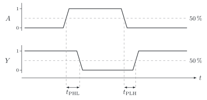
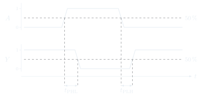
So far, our gates have been ideal. A real gate needs a short time until its output follows a change at its input, the propagation delay (German: Gatterlaufzeit) [5, p. 56]. It is measured from the moment the input has completed 50 % of its change in voltage to the moment the output has completed 50 % of its change [5, p. 57]. Since the two directions can differ, datasheets distinguish two values (figure): tPLH for an output that changes from LOW to HIGH and tPHL for an output that changes from HIGH to LOW [5, p. 57]. Often, they give a single value tpd; for the 74HC00, it is the larger of the two [11].
For the gates of the 74HC00 in complementary metal oxide semiconductor (CMOS) technology, the datasheet gives a propagation delay of typically 9 ns at a supply voltage of 4.5 V, and at most 18 ns at 25 °C [11].
Where does this time come from? The output of a gate is connected to the inputs of the following gates and to lines. Each input of a gate in this technology acts like a small capacitor [12, p. 41] – an input of the 74HC00 has typically 3 pF [11] – and the lines add further capacitance. When the output switches, the transistor that is switched on has to charge or discharge this capacitance, and it does so through its own resistance in the on state. As in every circuit of a resistor and a capacitor, this takes time; the switching time is approximately [12, p. 50]:
ts≈Ron⋅CL
where:
ts is the switching time in seconds (s)
Ron is the resistance of the switched-on transistor in ohms (Ω)
CL is the capacitance at the output of the gate, the load, in farads (F)
Fast circuits therefore need transistors with a low resistance in the on state and small capacitances at their outputs. And the faster a circuit switches, the more power it needs, because the capacitance is charged or discharged every time the output switches [12, p. 51]; this is the price of the low power at rest from section 1.1. What happens inside the semiconductor meanwhile goes beyond this module.
Why do a few nanoseconds matter? Signals often pass through several gates one after another, and their delays add up (section 6.3). And when two signals that should change at the same moment arrive at slightly different times, a short spurious pulse can appear at the output: a hazard, the topic of DET-04.
4 Inverted and exclusive – The derived operations NAND, NOR, XOR and XNOR
4.1 The NAND gate
The derived logic operations (German: abgeleitete Verknüpfungen) combine the basic operations. The NAND gate (German: NAND-Gatter) is an AND gate with an inverted output; the N stands for NOT [5, p. 47]. Its output is 0 only if all its inputs are 1:
A
B
Y
0
0
1
0
1
1
1
0
1
1
1
0
Y=A⋅B
where:
Y is the output, 0 or 1
A and B are the inputs, each 0 or 1
Read: ‘Y equals not A and B’. The bar covers the whole product, not the single variables: first A and B are combined, then the result is negated.
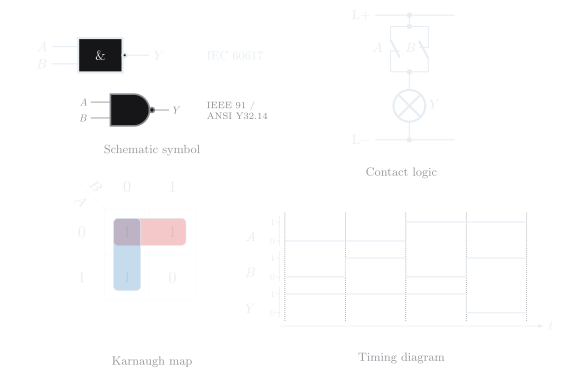
The symbol of the International Electrotechnical Commission (IEC) is the AND symbol with a negation circle at the output; the American symbol carries a small circle as well. In contact logic, two normally closed contacts lie in parallel: the lamp goes out only if both are actuated. The Karnaugh map has a single 0, and in VHDL, the operator is nand:
Y <= A nand B;
Why does a combination of AND and NOT have a gate of its own? Because complementary metal oxide semiconductor (CMOS) technology builds it directly. A NAND gate needs four transistors; an AND gate needs six, because it is a NAND gate followed by an inverter [5, pp. 64–66]. CMOS builds NOT, NAND and NOR directly [5, p. 64]. The integrated circuit in the photo in section 1.1 contains four NAND gates, and so does the 74HC00, whose datasheet we used in section 3.5 [11]. The NAND gate can even replace all other gates, as section 5.6 shows.
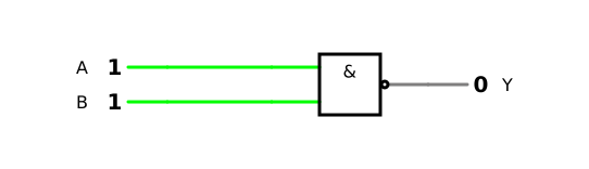
In the simulator, the output is 1 in three of the four combinations; it shows a 0 only when both inputs are 1.
4.2 The NOR gate
The NOR gate (German: NOR-Gatter) is an OR gate with an inverted output: its output is 1 only if all its inputs are 0 [5, pp. 47–48].
A
B
Y
0
0
1
0
1
0
1
0
0
1
1
0
Y=A+B
where:
Y is the output, 0 or 1
A and B are the inputs, each 0 or 1
Read: ‘Y equals not A or B’; the bar again covers the whole expression.
The IEC symbol is the OR symbol with a negation circle. In contact logic, two normally closed contacts lie in series: the lamp lights only if neither of them is actuated. The Karnaugh map has a single 1, in the cell for A=0 and B=0. In VHDL, the operator is nor:
Y <= A nor B;
Like the NAND gate, the NOR gate is built directly in CMOS [5, p. 68], and it, too, can replace all other gates [5, p. 111].
Our heat pump offers an example. It has an interface called Smart Grid Ready (SG Ready): two switching signals through which the energy supplier or an energy manager can influence how it runs [13]. If both signals are 0, the heat pump works in normal operation [13]. Normal operation therefore means: neither the first nor the second signal is 1 – a NOR of the two. Section 6.6 shows what the other three combinations mean.
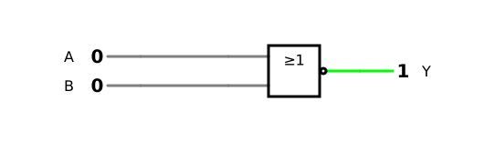
In the simulator, the output shows a 1 only as long as both inputs are 0.
4.3 The XOR gate
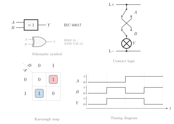
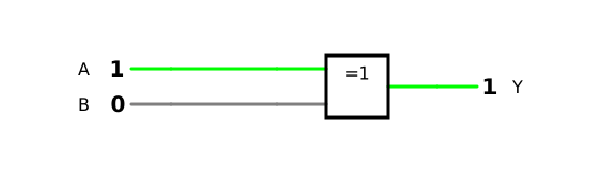
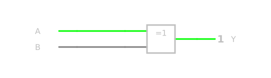
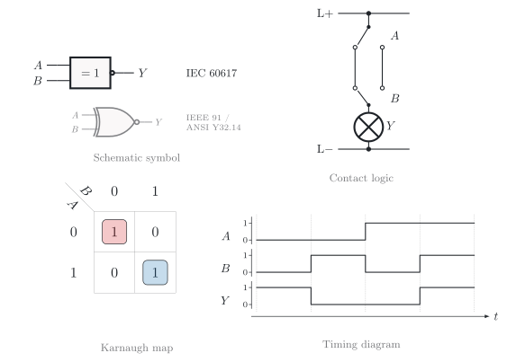
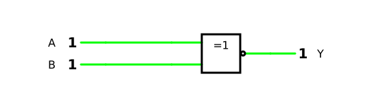
The XOR gate (German: XOR-Gatter), short for exclusive OR (German: Exklusiv-ODER, Antivalenz), delivers a 1 if its two inputs are different [5, p. 48], that is, if exactly one of them is 1. Unlike the OR gate, it delivers a 0 when both inputs are 1: one or the other, but not both.
A
B
Y
0
0
0
0
1
1
1
0
1
1
1
0
Y=A⊕B=A⋅B+A⋅B
where:
Y is the output, 0 or 1
A and B are the inputs, each 0 or 1
Read: ‘Y equals A exclusive-or B’. The right-hand side says the same with AND, OR and NOT: either A is 0 and B is 1, or A is 1 and B is 0.
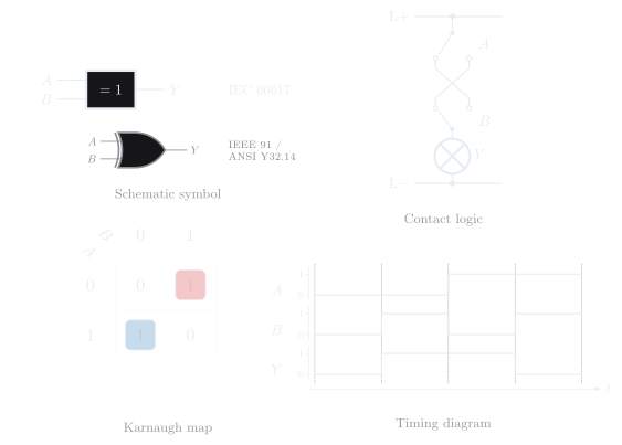
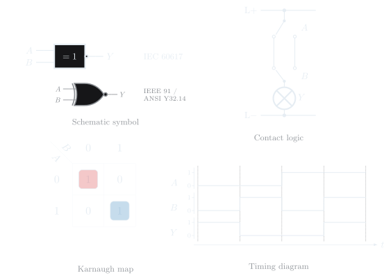
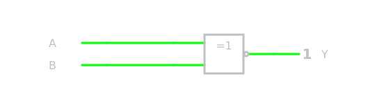
The IEC symbol carries the qualifying symbol =1 [12, p. 18], which states the rule: exactly one input is 1. The American symbol is the OR symbol with an additional curved line at the inputs. In this module, an XOR gate always has two inputs, in the simulator as well. In VHDL, the operator is xor:
Y <= A xor B;
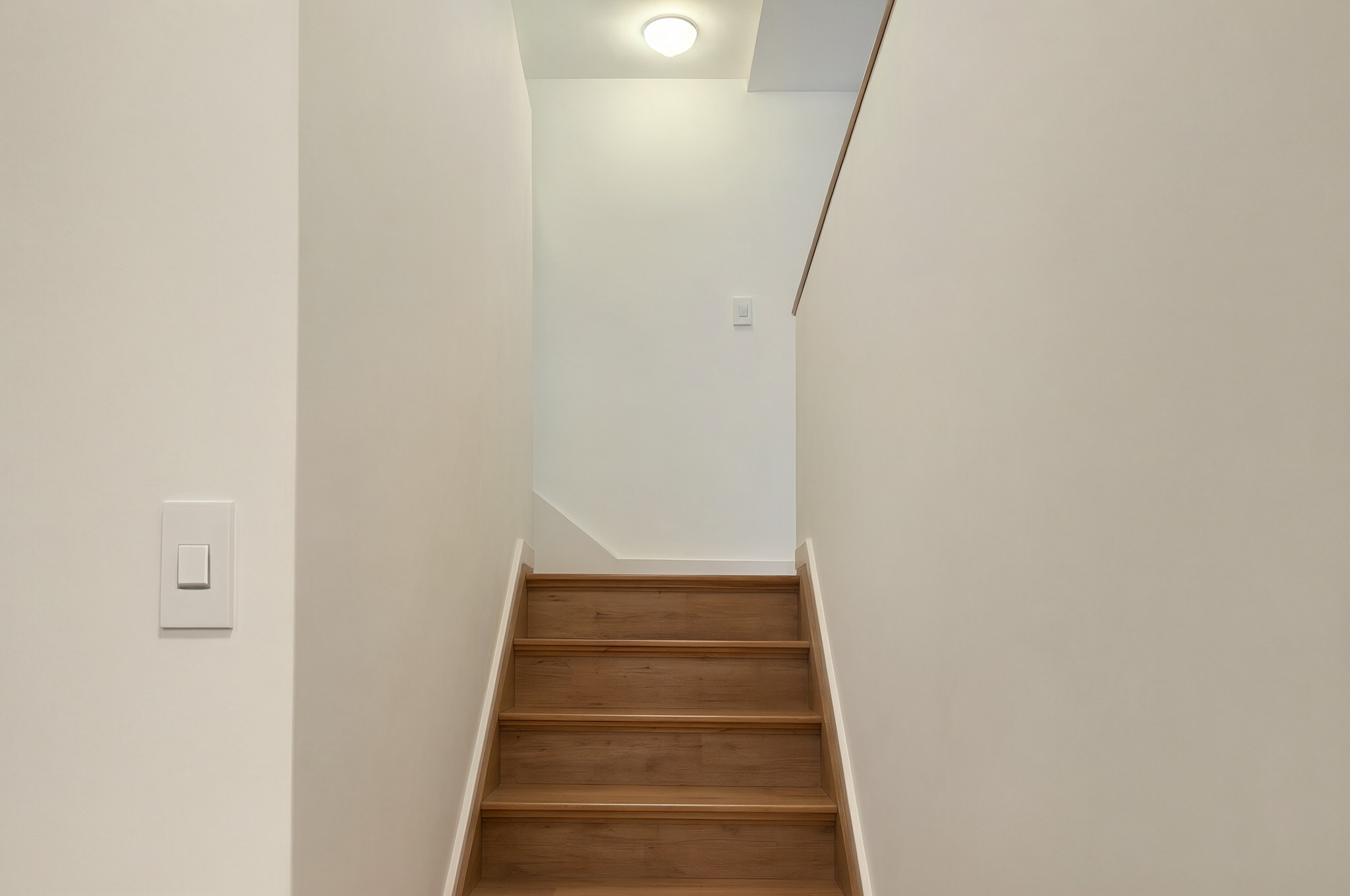
Contact logic shows the XOR in a circuit that you probably operate every day: the two-way switching (German: Wechselschaltung) of a staircase light. A switch at the foot of the stairs and one at the top each have a change-over contact (German: Wechsler), and every time you flip either of them, the light changes its state. If we call the position of each switch 0 or 1, the light is on when the two positions differ – an XOR. Whether it is on when they differ or when they are equal depends only on how the switches were mounted; in the second case, the circuit is an XNOR, our next gate.
Image by Qwen-Image 2.1
The XOR gate also appears wherever bits are added. Compare the table of binary addition in DET-01, 8.1: the column ‘Sum’ is exactly the XOR of A and B, and the column ‘Carry’ is their AND.
In the simulator, the output shows a 1 when the two inputs differ.
4.4 The XNOR gate
The XNOR gate (German: XNOR-Gatter) is an XOR gate with an inverted output: it delivers a 1 if its two inputs are equal [5, p. 49]. The XNOR operation is therefore also called equivalence (German: Äquivalenz).
A
B
Y
0
0
1
0
1
0
1
0
0
1
1
1
Y=A⊕B=A⋅B+A⋅B
where:
Y is the output, 0 or 1
A and B are the inputs, each 0 or 1
Read: ‘Y equals not A exclusive-or B’. The right-hand side says: either both are 1, or both are 0.
The IEC symbol for the XNOR gate is the XOR symbol with a negation circle at the output; the standard also has a symbol of its own for the equivalence, with the qualifying symbol =, which you will find in German textbooks [12, p. 18]. In contact logic, the two change-over contacts are wired so that the lamp lights when both are in the same position. The Karnaugh map has its two 1s on the diagonal. In VHDL, the operator is xnor:
Y <= A xnor B;
Wherever two bits have to agree, the XNOR gate checks it. A controller could, for example, compare the command to switch on a pump with the feedback signal from the pump: as long as both agree, the XNOR gate delivers a 1. If the pump does not follow its command, the gate delivers a 0, and the controller can report a fault.
In the simulator, the output shows a 1 when the two inputs are equal.
4.5 IEC and American symbols side by side
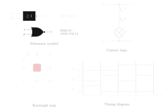
You now know all seven gates. The figure shows them in both sets of symbols. In the symbols of IEC 60617, the qualifying symbol states the rule by which the inputs are combined [12, pp. 16–18]:
1: the output follows its single input; with the negation circle, this is the inverter
&: all inputs are 1
≥1: at least one input is 1
=1: exactly one input is 1
A circle at the output negates it. This is how NAND, NOR and XNOR arise from AND, OR and XOR.
The American symbols, laid down by the Institute of Electrical and Electronics Engineers (IEEE) and the American National Standards Institute (ANSI) in IEEE 91 / ANSI Y32.14, give each operation a shape of its own instead: the D for AND, the curved shield for OR, the triangle for the inverter. A small circle, often called a bubble, negates here as well.
Why two sets of symbols? Europe and North America have each kept their own tradition. In this module, we use IEC 60617 for all circuits, in the exercises as well as in the simulator, which shows IEC symbols. You will meet the American symbols in English-language textbooks such as LaMeres [5], in many datasheets and in software tools; with this overview, you can translate them.
5 Calculating with 0 and 1 – Boolean algebra
5.1 Notations of Boolean algebra
With the seven gates, we can build any logic circuit. To design circuits and to minimize them, we now need rules for calculating with 0 and 1: Boolean algebra (German: Schaltalgebra). An algebra comprises the rules that apply to the operations of a number system [5, p. 93].
An algebra with two values
In 1854, the English mathematician Boole presented an algebra for a system with only two states, true and false [5, p. 93] – almost a century before the first electronic computers. Today, it is the mathematical basis of every digital circuit.
Boolean algebra is used in mathematics, computer science and electrical engineering, and each discipline has its own notation for the same operations. Mathematics calls the three basic operations conjunction (German: Konjunktion), disjunction (German: Disjunktion) and negation [5, p. 94]. You will meet all the notations sooner or later, so here they are side by side:
Operation
Mathematics and logic
Computer science
Electrical engineering
AND
A∧B
A && B or A & B
A⋅B or AB
OR
A∨B
A || B or A | B
A+B
NOT
¬A
!A or ~A
A or A′
NAND
¬(A∧B)
!(A && B)
A⋅B
NOR
¬(A∨B)
!(A || B)
A+B
XOR
A⊕B
A ^ B
A⊕B
XNOR
A⇔B
A == B
A⊕B
The truth values differ as well: mathematics and logic speak of true and false, computer science writes true and false, and electrical engineering uses 1 and 0, which stand for HIGH and LOW in positive logic.
In this module, we use the notation of electrical engineering: the dot for AND, which may be omitted, the plus sign for OR and the bar for NOT. It has a practical advantage: with the dot and the plus sign, many rules of Boolean algebra look like the familiar rules of school algebra. The following sections show where this similarity helps and where it misleads. LaMeres also writes the negation as a prime, A′, because it can be typed in any text editor [5, p. 46]; when you read his book, think of the prime as a bar.
5.2 Axioms and precedence
An axiom (German: Axiom) is a basic statement that is accepted without proof [5, p. 94]. Boolean algebra rests on five of them [5, pp. 94–95]:
A variable has one of two values: A=0 if A=1, and A=1 if A=0.
Negation: if A=0, then A=1, and if A=1, then A=0.
Logical product: A⋅B=1 if A=B=1, and A⋅B=0 otherwise.
Logical sum: A+B=1 if A=1 or B=1, and A+B=0 otherwise.
Precedence: NOT before AND, AND before OR.
The first four repeat in algebraic form what you know from the gates. The fifth, the precedence (German: Vorrang), states the order in which an expression is evaluated, just as multiplication comes before addition at school. Example:
Y=A⋅B+C=((A)⋅B)+C
where:
Y is the output, 0 or 1
A, B and C are the inputs, each 0 or 1
First A is negated, then the result is combined with B by AND, and finally the result is combined with C by OR [5, p. 95]. Parentheses state the order explicitly; they are needed wherever an OR is to be evaluated before an AND, as in (A+B)⋅C.
VHDL does not know this order. Only not takes precedence; and, or, nand, nor, xor and xnor all have the same rank [5, p. 172]. VHDL therefore does not accept an expression that mixes them without parentheses: Y <= A and B or C; is an error, Y <= (A and B) or C; is correct. NAND and NOR cannot even be chained without parentheses: A nor B nor C is not accepted either, because NOR, unlike OR, is not associative (section 5.4). Whenever you read VHDL, the parentheses show you the structure of the circuit.
Erratum in the textbook by LaMeres
LaMeres [5, p. 172] states that logical operators of the same rank are evaluated from left to right if there are no parentheses, and gives F5 <= H nor I nor J; and F6 <= K xor L xnor M; as examples. In fact, VHDL accepts neither: without parentheses, an expression may only chain the same operator, such as and, or, xor or xnor, and nand and nor cannot be chained at all.
5.3 Theorems with one variable
A theorem (German: Theorem) is a statement that has to be proved before it may be used [5, p. 95]. In Boolean algebra, proving is easy: since each variable can only be 0 or 1, we simply try all combinations. This is called a proof by exhaustion (German: vollständige Fallunterscheidung) [5, p. 95]. The theorems come in pairs, one for OR and one for AND [5, p. 96].
The first five theorems contain only one variable [5, pp. 98–100]:
Theorem
With OR
With AND
Identity
A+0=A
A⋅1=A
Null element
A+1=1
A⋅0=0
Idempotence
A+A=A
A⋅A=A
Complements
A+A=1
A⋅A=0
Involution, A=A
–
–
The names follow LaMeres: identity (German: Neutralitätsgesetz), null element (German: Extremalgesetz), idempotence (German: Idempotenzgesetz), complements (German: Komplementärgesetz) and involution (German: Doppelnegationsgesetz).
Contact logic makes them visible. A+1 is a contact in parallel with a plain wire: the lamp is always on. A⋅0 is a contact in series with an open line: the lamp is always off. And A⋅A is a normally open and a normally closed contact of the same switch in series: one of them is always open. As an example of a proof, the truth table of the complements theorem:
A
A
A+A
0
1
🟢1
1
0
🟢1
For every value of A, the result is 1; this proves A+A=1.
These theorems are useful in practice. If an input of an OR gate is permanently 0, it can be removed (identity) [5, p. 98]. An input that is permanently 1 forces an OR output to 1, and an input that is permanently 0 forces an AND output to 0 (null element); circuits use this to set or clear a value [5, p. 99]. And two inverters in a row cancel each other out (involution) [5, p. 100].
5.4 Theorems with several variables
The next five theorems contain two or three variables [5, pp. 100–105]:
Theorem
With OR
With AND
Commutative property
A+B=B+A
A⋅B=B⋅A
Associative property
(A+B)+C=A+(B+C)
(A⋅B)⋅C=A⋅(B⋅C)
Distributive property
A+B⋅C=(A+B)⋅(A+C)
A⋅(B+C)=A⋅B+A⋅C
Absorption
A+A⋅B=A
A⋅(A+B)=A
Uniting
A⋅B+A⋅B=A
(A+B)⋅(A+B)=A
The commutative property (German: Kommutativgesetz) says that the order of the inputs does not matter, which helps to untangle crossed wires [5, p. 100]. The associative property (German: Assoziativgesetz) says that the grouping does not matter. This is why an OR with twelve inputs may be built from smaller OR gates, as in section 3.4 [5, p. 102].
NAND and NOR are not associative
The associative property holds for AND and OR, but not for NAND and NOR [12, p. 20]. A NAND gate with three inputs is not the same as two NAND gates with two inputs each, connected one after the other.
With AND, the distributive property (German: Distributivgesetz) is familiar from school: multiplying out. With OR, A+B⋅C=(A+B)⋅(A+C), it has no counterpart in ordinary arithmetic and looks wrong at first sight; check it with a truth table. Absorption (German: Absorptionsgesetz) removes a term that another term already covers [5, p. 104]. Uniting (German: Zusammenfassen) removes a variable that has no influence: if a product appears once with B and once with B, B can go [5, pp. 104–105]. In DET-03, the Karnaugh map makes such pairs visible.
Theorems can also be proved with other theorems. Absorption, for example, follows from identity, the distributive property and the null element:
The most useful theorems for circuits go back to De Morgan, a British mathematician of Boole’s time [5, p. 95]. De Morgan’s laws (German: De-morgansche Gesetze) state [5, p. 105]:
A⋅BA+B=A+B=A⋅B
where:
A and B are any logic variables, each 0 or 1
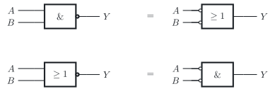
Read: ‘not A and B equals not A or not B’, and ‘not A or B equals not A and not B’. In terms of gates: a NAND gate is an OR gate with inverted inputs, and a NOR gate is an AND gate with inverted inputs (figure).
The truth table proves the first law:
A
B
A⋅B
A⋅B
A
B
A+B
0
0
0
🟢1
1
1
🟢1
0
1
0
🟢1
1
0
🟢1
1
0
0
🟢1
0
1
🟢1
1
1
1
🟢0
0
0
🟢0
The fourth and the last column agree in every row. A rule of thumb helps with longer expressions: break the bar and change the operator [5, p. 108]. Where a long bar is split into shorter ones, the operator below the break changes from AND to OR or from OR to AND.
Our smartphone display shows what the law means. In section 2.1, the display is off when Y=A⋅B=1. When is it on? The negation gives Y=A⋅B=A+B: the display is on if no call is active or if the sensor is not covered – exactly what you would say in words.
De Morgan’s laws bridge Boolean algebra and the hardware [5, p. 106]. We design with AND, OR and NOT, because these are easy to think in. Complementary metal oxide semiconductor (CMOS) technology, however, builds NOT, NAND and NOR directly. With De Morgan’s laws, every design with AND and OR can be converted into one with NAND and NOR gates.
5.6 Transforming expressions step by step
With the theorems, an expression can be transformed into another one that describes the same function, usually a shorter one that needs fewer gates. As an example, take the screen of the smartphone from section 3.3. Someone who describes it case by case writes: the screen switches on if the phone is lifted without the button being pressed, or if the button is pressed without the phone being lifted, or if both happen. With A for ‘power button pressed’ and B for ‘phone lifted’:
Y=A⋅B+A⋅B+A⋅B=A⋅B+A⋅B+A⋅B+A⋅B=B⋅(A+A)+A⋅(B+B)=B⋅1+A⋅1=A+Bidempotence, commutative propertycommutative and distributive propertiescomplementsidentity, commutative property
where:
Y is the output ‘screen on’, 0 or 1
A is the input ‘power button pressed’, 0 or 1
B is the input ‘phone lifted’, 0 or 1
The trick lies in the second line: by idempotence, A⋅B=A⋅B+A⋅B, so that the term can be used twice. Three AND gates, two inverters and an OR gate with three inputs become a single OR gate – the gate of section 3.3. Check such a result with a truth table, as in section 5.3.
A set of operations is functionally complete (German: funktional vollständig) if every logic function can be built with it [5, p. 110]. AND, OR and NOT form such a set. NAND alone is functionally complete as well [5, p. 110]:
AA⋅BA+B=A⋅A=A⋅B=A⋅B
where:
A and B are any logic variables, each 0 or 1
The first line is a NAND gate with both inputs connected (idempotence): an inverter. The second is a NAND gate followed by such an inverter (involution): an AND gate. The third is a NAND gate with inverted inputs (De Morgan): an OR gate. The same works with NOR alone [5, p. 111]. Sheffer proved as early as 1913 that the whole of Boolean algebra can be built on a single such operation.
6 What does this circuit do? – Analysis of given circuits
6.1 From the circuit to the expression
With the gates and the rules, we can now analyse circuits that someone else has designed and find out what they do. This is useful when you look for a fault, check a design or want to understand a circuit you did not design yourself [5, p. 111]. The analysis yields the logic expression, the truth table and the timing behaviour of the circuit.
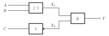
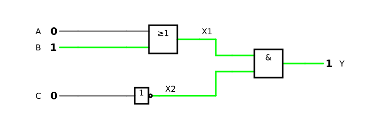
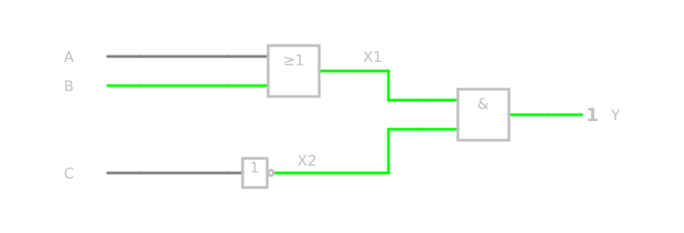
Our example is again the display of the smartphone (figure). Inputs A and B come from the power button and from lifting the phone, as in section 3.3; input C reports that the proximity sensor is covered during a call, as in section 2.1. The circuit has three gates and two intermediate nodes, X1 and X2.
The procedure has two steps [5, pp. 111–112]:
Label every intermediate node, that is, every output of a gate inside the circuit.
Write down the expression of each node, from the inputs on the left to the output on the right, each from the expressions of the nodes before it.
For our circuit:
X1X2Y=A+B=C=X1⋅X2=(A+B)⋅C
where:
A is the input ‘power button pressed’, 0 or 1
B is the input ‘phone lifted’, 0 or 1
C is the input ‘proximity sensor covered during a call’, 0 or 1
X1 and X2 are the intermediate nodes, each 0 or 1
Y is the output ‘display on’, 0 or 1
The parentheses are necessary: without them, AND would take precedence over OR (section 5.2). Read as a sentence: the display switches on if the power button is pressed or the phone is lifted, and the proximity sensor is not covered during a call. So if you press the button with your ear during a call, the display stays dark.
6.2 From the circuit to the truth table
The truth table follows in the same way. For each combination of the inputs, the nodes are evaluated from left to right, each from the values of the nodes before it [5, p. 112]. Columns for the intermediate nodes keep track of the calculation:
A
B
C
X1=A+B
X2=C
Y=X1⋅X2
0
0
0
0
1
0
0
0
1
0
0
0
0
1
0
1
1
1
0
1
1
1
0
0
1
0
0
1
1
1
1
0
1
1
0
0
1
1
0
1
1
1
1
1
1
1
0
0
The output is 1 in rows 2, 4 and 6, counting from row 0: exactly where at least one of A and B is 1 and C is 0. The expression from section 6.1 says the same. The truth table is the safest way to check an analysis, because it leaves no combination out; with three inputs, it has eight rows, with four inputs already sixteen. The columns of the intermediate nodes also help to find a fault: if a real circuit behaves differently from the table, measure the nodes one after another and compare them with their columns.
In the simulator, you can switch the three inputs through all eight combinations and compare each result with a row of the table.
6.3 Timing behaviour of a circuit
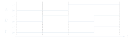
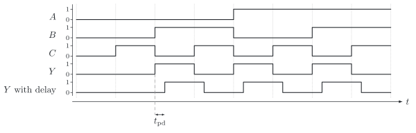
The timing diagram (figure) shows the circuit when the inputs run through all eight combinations in the order of the truth table. In the ideal diagram, the output follows the inputs without delay; it is 1 in the intervals 2, 4 and 6, counted from 0 like the rows of the truth table.
In a real circuit, each gate adds its propagation delay. A change at an input reaches the output along a path through several gates, and the delay of a path is the sum of the propagation delays of the gates on it. The delay of the whole circuit is the delay of its longest path, because only after this time is the output valid for every change of the inputs [5, p. 113].
You find it stage by stage, from the inputs to the output. A gate can switch only when the slowest of its inputs has arrived; the delay at its output is therefore the largest delay at its inputs plus its own propagation delay. In our circuit, the OR gate and the inverter form the first stage and work at the same time; the AND gate forms the second stage and has to wait for the slower of the two:
tpd,circuit=max(tpd,OR,tpd,NOT)+tpd,AND
where:
tpd,circuit is the propagation delay of the whole circuit in seconds (s)
tpd,OR and tpd,NOT are the propagation delays of the OR gate and the inverter in the first stage, in seconds (s)
tpd,AND is the propagation delay of the AND gate in the second stage, in seconds (s)
The circuit has three inputs, but its longest path passes through only two gates, so two delays are added. If we assume, for simplicity, that each gate has a propagation delay of 9 ns, the typical value of the NAND gates of the 74HC00 [11], then:
tpd,circuit=max(9ns,9ns)+9ns=18ns
Only 18 ns after a change at the inputs is the output of our circuit valid. In the timing diagram, the output with delay is therefore shifted to the right. Before this time has passed, the output can briefly show a wrong value when several inputs change at once and their changes arrive one after another. Such hazards are the topic of DET-04.
6.4 From VHDL code to the circuit
A design in VHDL can be analysed in the same way. The entity shows the inputs and outputs, and each assignment of the architecture shows a gate [5, pp. 168–171]. Example:
entity display_on is port (A, B, C : in bit; -- A: power button, B: phone lifted, C: covered in a call Y : out bit); -- Y: display onend entity;architecture behaviour of display_on is signal X1, X2 : bit; -- intermediate nodesbegin X1 <= A or B; X2 <= not C; Y <= X1 and X2;end architecture;
The procedure:
Read the ports of the entity: A, B and C are inputs, Y is the output.
Read the signals declared before begin: X1 and X2 are intermediate nodes inside the circuit [5, p. 169].
Turn each operator into a gate: or into an OR gate, not into an inverter, and into an AND gate.
Draw the gates from left to right and connect them by their names.
The result is the circuit of section 6.1. The order of the three assignments does not matter: they are concurrent, and if you swap them, they still describe the same hardware [5, p. 174]. The same circuit can also be written in a single line, Y <= (A or B) and not C;. Here, the parentheses are required, because VHDL does not accept mixed operators without them (section 5.2).
When you read VHDL, look out for three things: the names of the ports, the operators and the parentheses. Everything else, such as the keywords entity, architecture, begin and end, is the frame that every design has.
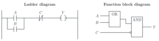
6.5 The same circuit in a programmable logic controller
In industry, many controls are not built from gates but programmed on a programmable logic controller (PLC), such as the one you met in DET-01, 6.3. The International Electrotechnical Commission (IEC) defines its programming languages in the standard IEC 61131-3 [14]. Two of them are graphical and resemble forms that you already know (figure):
The ladder diagram (LD, German: Kontaktplan, KOP) is contact logic turned by 90 degrees: two vertical rails on the left and right, contacts on the horizontal rungs between them, and a coil as the output. Our display circuit has A and B as normally open contacts in parallel, in series with a normally closed contact C, and the coil Y.
The function block diagram (FBD, German: Funktionsbausteinsprache, FBS) connects function blocks that resemble the schematic symbols: an OR block with A and B, an AND block with the result and the negated C.
A third, older language is the instruction list (IL, German: Anweisungsliste, AWL), a text close to the machine that processes one instruction per line. For our circuit, it loads A, combines it with B by OR and with the negated C by AND, and stores the result in Y:
LD A (* load A *)OR B (* OR with B *)ANDN C (* AND with NOT C *)ST Y (* store the result in Y *)
The current edition of the standard from 2025 names structured text, a language similar to a programming language, together with the ladder diagram and the function block diagram as its languages [14]; the instruction list is no longer among them, but older controllers still use it. We show these languages only this once: they connect what you learn here with the programming of controllers. In the following lessons, we work with the seven forms of chapter 2.
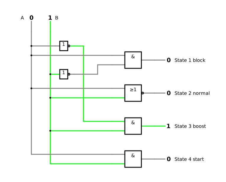
6.6 Two bits, four operating states
Now we can answer the last guiding question. Our heat pump has the interface Smart Grid Ready (SG Ready), which the German Heat Pump Association (Bundesverband Wärmepumpe) has defined [13]. Through two switching signals, the energy supplier or an energy manager can influence how the heat pump runs. In the version with four states, the two signals give four operating states [13]. We call the signals A and B, in the order in which they are written as a pair A:B:
A
B
State
Meaning
0
0
2
normal operation
0
1
3
boost: a recommendation to switch on, with increased set points for heating and hot water
1
0
1
block: the heat pump must not start, for at most two hours
1
1
4
start command
Read as a truth table, the table has four outputs, one for each state, and in each row, exactly one of them is 1. Each state is therefore recognized by a single gate that combines the two signals or their negations:
A and B are the first and the second switching signal, each 0 or 1
Y1 to Y4 are the outputs for the operating states 1 to 4, each 0 or 1
Normal operation is the NOR gate from section 4.2, the start command is an AND gate, and the two other states are AND gates with one inverted input. The simulation shows the complete circuit.
Analyse the circuit in the simulator: switch A and B through all four combinations and check that exactly one output shows a 1 each time. In our example system, an energy manager selects state 3 when the photovoltaic system feeds surplus power into the power grid; the heat pump then raises its set point for hot water and stores the surplus energy as heat. In DET-05, you will meet a standard component that does exactly this job, the decoder, and see how state 4 can be locked out.
7 What have you learnt? – Summary and answers to the guiding questions
7.1 The building blocks of knowledge
Basic gates and derived logic operations: NOT, AND and OR are the basic operations; NAND, NOR, XOR and XNOR are derived from them. Complementary metal oxide semiconductor (CMOS) technology builds NOT, NAND and NOR directly from transistors that work as switches.
Schematic symbols: The standard of the International Electrotechnical Commission (IEC), IEC 60617, draws each gate as a rectangle with a qualifying symbol – 1, &, ≥1 or =1 – and negates with a circle. The American symbols give each gate a shape of its own. In this module, we use IEC 60617.
Seven forms of representation: schematic symbol, contact logic, truth table, logic expression, VHDL code, Karnaugh map and timing diagram describe the same function, each for its own purpose.
Analysis of given circuits: Label the intermediate nodes and work from the inputs to the output to find the expression and the truth table; the longest path determines the delay. VHDL code becomes a circuit by turning each operator into a gate.
Rules of Boolean algebra and its notations: Five axioms and theorems in pairs, one for OR and one for AND, among them De Morgan’s laws, transform expressions. Mathematics, computer science and electrical engineering write the same operations in different notations.
Propagation delay: A real gate needs a few nanoseconds to switch, because its transistors have to charge or discharge the capacitances at its output.
7.2 Answers to the guiding questions
A car has four doors and a boot: which logic switches on the interior light if any of them is opened?
An OR operation with five inputs. Each door and the boot has a contact that delivers a 1 when it is open, and the interior light is on as soon as at least one input is 1: Y=A+B+C+D+E. In contact logic, the five contacts lie in parallel.
Why does a single warning lamp light up as soon as any one of a dozen faults occurs?
Because the lamp shows the OR of all fault bits, the collective fault. As soon as any one of the twelve bits is 1, the OR output is 1 and the lamp lights up, whichever fault it is. Since a single gate has a limited number of inputs, the OR of twelve inputs can be built from several smaller OR gates; the associative property allows this.
With just two signals, the energy supplier can make a heat pump pause, run normally or step up its heating – how does that work?
Two bits give 22=4 combinations, and Smart Grid Ready (SG Ready) assigns an operating state to each of them: 0:0 normal operation, 0:1 boost, 1:0 block and 1:1 start command. Each state is recognized by a single gate: normal operation by a NOR gate, the start command by an AND gate, block and boost by AND gates with one inverted input.
Where do I look things up? – Sources and references
All sources that I cite in this script with a number in square brackets, such as [5], are listed on the page References. There you will also find the books that I recommend for looking things up, the image licences and a note on the use of AI.