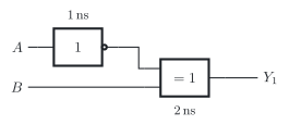
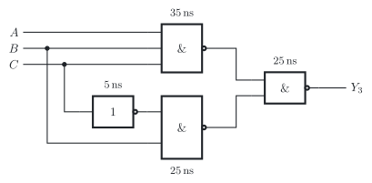
The four circuits below come from the textbook by LaMeres [5, pp. 146–147]; here they are drawn according to the standard of the International Electrotechnical Commission (IEC), IEC 60617. The number next to each gate is its propagation delay. In each circuit, label the intermediate nodes first, that is, the outputs of the gates inside the circuit.
Circuit 1 has the inputs A and B and the output Y1.
a) Determine the logic expression of the output Y1 of circuit 1.
b) Set up the truth table of circuit 1, with a column for each intermediate node.
c) Determine the propagation delay of circuit 1.
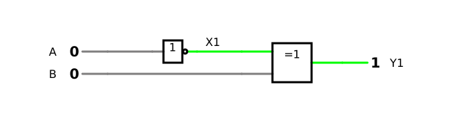
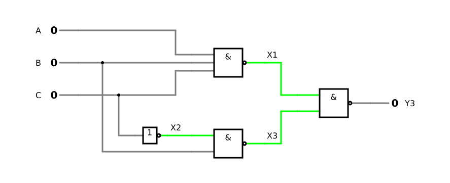
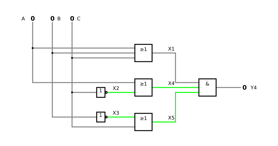
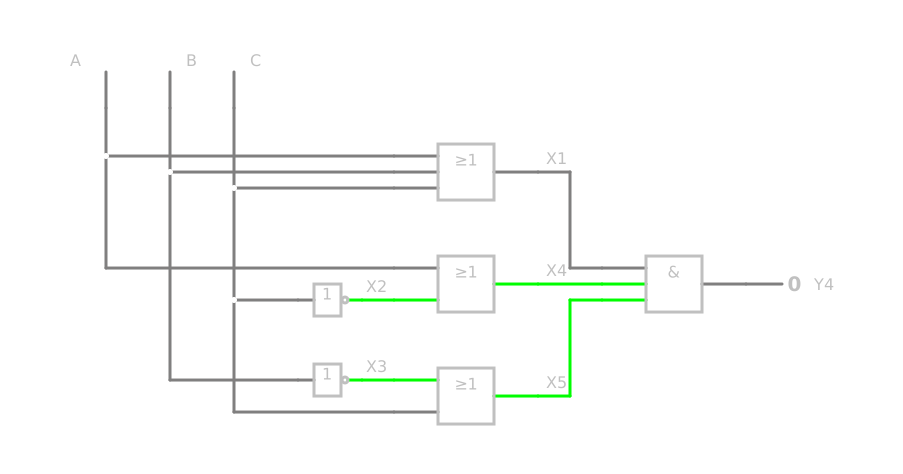
Check your truth table of b) in the simulation of circuit 1 by switching the inputs through all combinations.
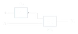
Circuit 1 [5, Fig. 4.27]: an inverter (1 ns) and an XOR gate (2 ns); inputs A and B, output Y1
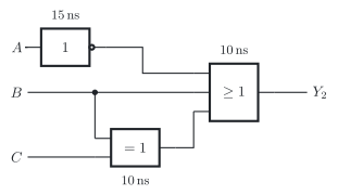
Circuit 2 [5, Fig. 4.28]: an inverter (15 ns), an XOR gate (10 ns) and an OR gate with three inputs (10 ns); inputs A, B and C, output Y2
Circuit 3 [5, Fig. 4.29]: a NAND gate with three inputs (35 ns), an inverter (5 ns) and two NAND gates with two inputs (25 ns each); inputs A, B and C, output Y3
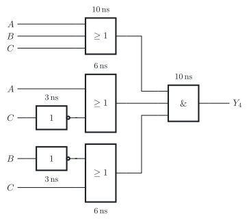
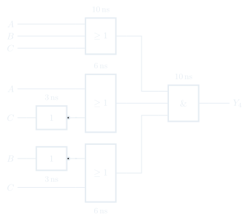
Circuit 4 [5, Fig. 4.31]: an OR gate with three inputs (10 ns), two inverters (3 ns each), two OR gates with two inputs (6 ns each) and an AND gate with three inputs (10 ns); inputs A, B and C, output Y4
Known:
Analysis of a circuit: label every intermediate node, then write down the expression of each node from the inputs to the output (DET-02)
Truth table with 2n rows and a column for each intermediate node, evaluated from left to right (DET-02)
Expressions of the gates, among them the XOR gate, A⊕B=A⋅B+A⋅B (DET-02), and the XNOR gate, A⊕B=A⋅B+A⋅B (DET-02)
De Morgan’s laws, A⋅B=A+B (DET-02), and involution, A=A (DET-02)
Propagation delay of a circuit, stage by stage: a gate switches only when the slowest of its inputs has arrived, so that the delay at its output is the largest delay at its inputs plus its own propagation delay; the delay of the circuit is that of its longest path (DET-02)
Required
a), d), g) and j) the logic expressions of Y1 to Y4
b), e), h) and k) the truth tables of the four circuits
c), f), i) and l) the propagation delays of the four circuits
a) Expression of circuit 1
Circuit 1 has one intermediate node, the output of the inverter; we call it X1. From the inputs to the output, each node follows from the nodes before it (DET-02, 6.1):
X1Y1=A=X1⊕B=A⊕B
Read: ‘Y1 equals A bar exclusive-or B’.
b) Truth table of circuit 1
With two inputs, the table has 22=4 rows, numbered from row 0 to row 3. In each row, we evaluate the nodes from left to right (DET-02, 6.2):
A
B
X1=A
Y1=X1⊕B
0
0
1
1
0
1
1
0
1
0
0
0
1
1
0
1
Y1 is 1 in rows 0 and 3, where A and B are equal: circuit 1 works like an XNOR gate.
Check with the expressions of the XOR gate and of the XNOR gate (DET-02, 4.3, DET-02, 4.4):
A⊕B=A⋅B+A⋅B=A⋅B+A⋅B=A⊕B
The expression of circuit 1 is that of the XNOR gate ✓
c) Propagation delay of circuit 1
Stage by stage from the inputs to the output, each node is valid after the largest delay at the inputs of its gate plus the delay of the gate itself; the inputs are valid from the start, after 0 ns (DET-02, 6.3):
The XOR gate at the output waits for the slowest of its inputs, X1 after 1 ns; B is valid at once. The propagation delay of circuit 1 is therefore tpd,circuit=3ns.
Check along all paths from an input to the output:
A → inverter → XOR gate: 1ns+2ns=3ns
B → XOR gate: 2ns
The longest path takes 3 ns ✓
Propagation delays in the simulator
The gates of the simulations have no propagation delay: the simulator shows only the logic of the circuits, like the ideal timing diagrams of the lesson (DET-02, 2.7). The propagation delays of the figures apply to the calculations in c), f), i) and l).
d) Expression of circuit 2
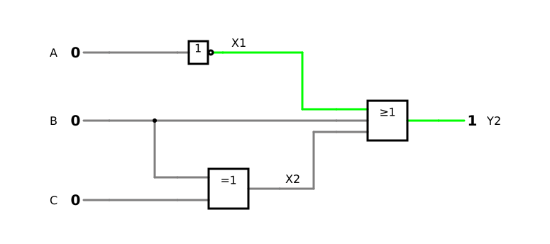
Circuit 2 has two intermediate nodes: X1 at the output of the inverter and X2 at the output of the XOR gate. Input B leads both to the XOR gate and directly to the OR gate:
X1X2Y2=A=B⊕C=X1+B+X2=A+B+(B⊕C)
The parentheses around B⊕C show that the XOR gate is evaluated before the OR gate.
e) Truth table of circuit 2
With three inputs, the table has 23=8 rows:
A
B
C
X1=A
X2=B⊕C
Y2=X1+B+X2
0
0
0
1
0
1
0
0
1
1
1
1
0
1
0
1
1
1
0
1
1
1
0
1
1
0
0
0
0
0
1
0
1
0
1
1
1
1
0
0
1
1
1
1
1
0
0
1
Y2 is 0 only in row 4, for A=1, B=0 and C=0: only there are all three inputs of the OR gate 0.
Check of row 4 with the expression. For A=1, B=0 and C=0:
Y2=A+B+(B⊕C)=1+0+(0⊕0)=0+0+0=0
✓
A gate too many
The table has a single 0, in row 4. The expression A+B+C is 0 in exactly this row as well, so that A+B+(B⊕C)=A+B+C: circuit 2 would work without its XOR gate. How to find such simplifications systematically is the topic of DET-03.
f) Propagation delay of circuit 2
Stage by stage from the inputs to the output, each node is valid after the largest delay at the inputs of its gate plus the delay of the gate itself; the inputs are valid from the start, after 0 ns:
The OR gate with three inputs at the output waits for the slowest of its inputs, X1 after 15 ns; X2 is valid after 10 ns and B is valid at once. The propagation delay of circuit 2 is therefore tpd,circuit=25ns.
Check along all paths from an input to the output:
A → inverter → OR gate with three inputs: 15ns+10ns=25ns
B or C → XOR gate → OR gate with three inputs: 10ns+10ns=20ns
B → OR gate with three inputs: 10ns
The longest path takes 25 ns ✓
g) Expression of circuit 3
Circuit 3 has three intermediate nodes: X1 at the output of the NAND gate with three inputs, X2 at the output of the inverter and X3 at the output of the NAND gate with two inputs in front:
Y3 is 1 if A, B and C are all 1 or if B is 1 and C is 0. The two NAND gates in front and the NAND gate at the output do the same as two AND gates followed by an OR gate. This is why NAND gates alone can replace AND and OR gates (DET-02, 5.6).
h) Truth table of circuit 3
A
B
C
X1=A⋅B⋅C
X2=C
X3=X2⋅B
Y3=X1⋅X3
0
0
0
1
1
1
0
0
0
1
1
0
1
0
0
1
0
1
1
0
1
0
1
1
1
0
1
0
1
0
0
1
1
1
0
1
0
1
1
0
1
0
1
1
0
1
1
0
1
1
1
1
0
0
1
1
Y3 is 1 in rows 2, 6 and 7.
Check with the result of g): A⋅B⋅C is 1 in row 7, B⋅C in rows 2 and 6; together, these are the rows 2, 6 and 7 ✓
i) Propagation delay of circuit 3
Stage by stage from the inputs to the output, each node is valid after the largest delay at the inputs of its gate plus the delay of the gate itself; the inputs are valid from the start, after 0 ns:
The NAND gate at the output waits for the slowest of its inputs, X1 after 35 ns; X3 is valid after 30 ns. The propagation delay of circuit 3 is therefore tpd,circuit=60ns.
Check along all paths from an input to the output:
A, B or C → NAND gate with three inputs → NAND gate: 35ns+25ns=60ns
C → inverter → NAND gate → NAND gate: 5ns+25ns+25ns=55ns
B → NAND gate → NAND gate: 25ns+25ns=50ns
The longest path takes 60 ns ✓ – it passes only two gates, whereas the path through three gates, C → inverter → NAND gate → NAND gate, takes only 55 ns.
j) Expression of circuit 4
Circuit 4 has five intermediate nodes: X1 at the output of the OR gate with three inputs, X2 and X3 at the outputs of the two inverters, and X4 and X5 at the outputs of the two OR gates with two inputs:
The AND gate combines three ORs. The parentheses are necessary, because AND takes precedence over OR (DET-02, 5.2).
k) Truth table of circuit 4
A
B
C
X1=A+B+C
X2=C
X3=B
X4=A+X2
X5=X3+C
Y4=X1⋅X4⋅X5
0
0
0
0
1
1
1
1
0
0
0
1
1
0
1
0
1
0
0
1
0
1
1
0
1
0
0
0
1
1
1
0
0
0
1
0
1
0
0
1
1
1
1
1
1
1
0
1
1
0
1
1
1
1
1
1
0
1
1
0
1
0
0
1
1
1
1
0
0
1
1
1
Y4 is 1 in rows 4, 5 and 7.
Check: the AND gate delivers a 0 wherever one of its three inputs is 0. The three ORs are 0 in these rows: A+B+C in row 0, A+C in rows 1 and 3 and B+C in rows 2 and 6. The remaining rows 4, 5 and 7 give 1 ✓
l) Propagation delay of circuit 4
Stage by stage from the inputs to the output, each node is valid after the largest delay at the inputs of its gate plus the delay of the gate itself; the inputs are valid from the start, after 0 ns:
The AND gate with three inputs at the output waits for the slowest of its inputs, X1 after 10 ns; X4 and X5 are valid after 9 ns. The propagation delay of circuit 4 is therefore tpd,circuit=20ns.
Check along all paths from an input to the output:
A, B or C → OR gate with three inputs → AND gate with three inputs: 10ns+10ns=20ns
B → inverter → OR gate → AND gate with three inputs: 3ns+6ns+10ns=19ns
C → inverter → OR gate → AND gate with three inputs: 3ns+6ns+10ns=19ns
A → OR gate → AND gate with three inputs: 6ns+10ns=16ns
C → OR gate → AND gate with three inputs: 6ns+10ns=16ns
The longest path takes 20 ns ✓ – it passes only two gates, whereas the two paths through three gates take only 19 ns.