
Prof. Dr. Thorsten Jungmann (last updated 2026-10-12)
Relates to DET-02 Logic operations
Task
The four circuits below come from the textbook by LaMeres [5, pp. 146–147]; here they are drawn according to the standard of the International Electrotechnical Commission (IEC), IEC 60617. The number next to each gate is its propagation delay. In each circuit, label the intermediate nodes first, that is, the outputs of the gates inside the circuit.
Circuit 1 has the inputs and and the output .
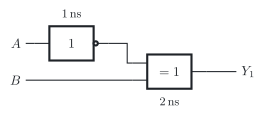
a) Determine the logic expression of the output of circuit 1.
b) Set up the truth table of circuit 1, with a column for each intermediate node.
c) Determine the propagation delay of circuit 1.
Check your truth table of b) in the simulation of circuit 1 by switching the inputs through all combinations.
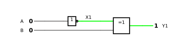
Circuit as text (File → Import From Text…)
<cir f="1" ts="0.000005" ic="1.500424758475255" cb="50" pb="50" vr="5" mts="5e-11">
  <Xor x="320 160 464 160" f="0" o="5"/>
  <I x="192 144 256 144" f="0" sl="0.5" hi="5"/>
  <L x="128 144 80 144" f="2"/>
  <L x="128 176 80 176" f="2"/>
  <w x="128 144 192 144" f="0"/>
  <w x="256 144 320 144" f="0"/>
  <w x="128 176 320 176" f="0"/>
  <M x="464 160 512 160" f="2"/>
  <x x="44 150 54 153" f="0" si="16" te="A"/>
  <x x="44 182 54 185" f="0" si="16" te="B"/>
  <x x="268 136 287 139" f="0" si="16" te="X1"/>
  <x x="532 166 551 169" f="0" si="16" te="Y1"/>
</cir>
Circuit 2 has the inputs , and and the output .
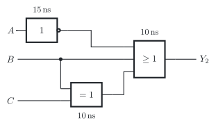
d) Determine the logic expression of the output of circuit 2.
e) Set up the truth table of circuit 2, with a column for each intermediate node.
f) Determine the propagation delay of circuit 2.
Check your truth table of e) in the simulation of circuit 2 by switching the inputs through all combinations.
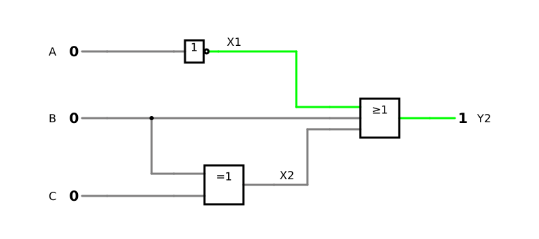
Circuit as text (File → Import From Text…)
<cir f="1" ts="0.000005" ic="1.500424758475255" cb="50" pb="50" vr="5" mts="5e-11">
  <Or x="448 192 592 192" f="0" in="3" o="5"/>
  <I x="224 96 288 96" f="0" sl="0.5" hi="5"/>
  <Xor x="224 288 368 288" f="0"/>
  <L x="128 96 80 96" f="2"/>
  <L x="128 192 80 192" f="2"/>
  <L x="128 304 80 304" f="2"/>
  <w x="128 96 224 96" f="0"/>
  <w x="288 96 400 96" f="0"/>
  <w x="400 96 400 176" f="0"/>
  <w x="400 176 448 176" f="0"/>
  <w x="128 192 192 192" f="0"/>
  <w x="192 192 448 192" f="0"/>
  <w x="192 192 192 272" f="0"/>
  <w x="192 272 224 272" f="0"/>
  <w x="128 304 224 304" f="0"/>
  <w x="368 288 416 288" f="0"/>
  <w x="416 288 416 208" f="0"/>
  <w x="416 208 448 208" f="0"/>
  <M x="592 192 640 192" f="2"/>
  <x x="44 102 54 105" f="0" si="16" te="A"/>
  <x x="44 198 54 201" f="0" si="16" te="B"/>
  <x x="44 310 55 313" f="0" si="16" te="C"/>
  <x x="300 88 319 91" f="0" si="16" te="X1"/>
  <x x="376 280 395 283" f="0" si="16" te="X2"/>
  <x x="660 198 679 201" f="0" si="16" te="Y2"/>
</cir>
Circuit 3 has the inputs , and and the output .
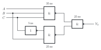
g) Determine the logic expression of the output of circuit 3.
h) Set up the truth table of circuit 3, with a column for each intermediate node.
i) Determine the propagation delay of circuit 3.
Check your truth table of h) in the simulation of circuit 3 by switching the inputs through all combinations.
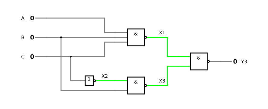
Circuit as text (File → Import From Text…)
<cir f="1" ts="0.000005" ic="1.500424758475255" cb="50" pb="50" vr="5" mts="5e-11">
  <Nand x="352 112 496 112" f="0" in="3" o="5"/>
  <I x="240 256 304 256" f="0" sl="0.5" hi="5"/>
  <Nand x="352 272 496 272" f="0" o="5"/>
  <Nand x="560 192 704 192" f="0"/>
  <L x="128 48 80 48" f="2"/>
  <L x="128 112 80 112" f="2"/>
  <L x="128 176 80 176" f="2"/>
  <w x="128 48 320 48" f="0"/>
  <w x="320 48 320 96" f="0"/>
  <w x="320 96 352 96" f="0"/>
  <w x="128 112 176 112" f="0"/>
  <w x="176 112 352 112" f="0"/>
  <w x="176 112 176 288" f="0"/>
  <w x="176 288 352 288" f="0"/>
  <w x="128 176 208 176" f="0"/>
  <w x="208 176 320 176" f="0"/>
  <w x="320 176 320 128" f="0"/>
  <w x="320 128 352 128" f="0"/>
  <w x="208 176 208 256" f="0"/>
  <w x="208 256 240 256" f="0"/>
  <w x="304 256 352 256" f="0"/>
  <w x="496 112 528 112" f="0"/>
  <w x="528 112 528 176" f="0"/>
  <w x="528 176 560 176" f="0"/>
  <w x="496 272 528 272" f="0"/>
  <w x="528 272 528 208" f="0"/>
  <w x="528 208 560 208" f="0"/>
  <M x="704 192 752 192" f="2"/>
  <x x="44 54 54 57" f="0" si="16" te="A"/>
  <x x="44 118 54 121" f="0" si="16" te="B"/>
  <x x="44 182 55 185" f="0" si="16" te="C"/>
  <x x="500 102 519 105" f="0" si="16" te="X1"/>
  <x x="310 246 329 249" f="0" si="16" te="X2"/>
  <x x="500 262 519 265" f="0" si="16" te="X3"/>
  <x x="772 198 791 201" f="0" si="16" te="Y3"/>
</cir>
Circuit 4 has the inputs , and and the output .
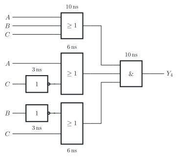
j) Determine the logic expression of the output of circuit 4.
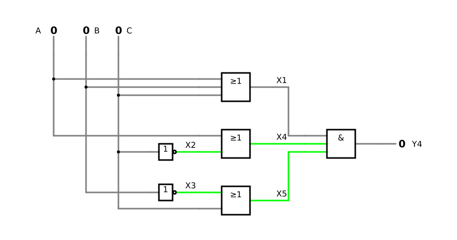
k) Set up the truth table of circuit 4, with a column for each intermediate node.
l) Determine the propagation delay of circuit 4.
Check your truth table of k) in the simulation of circuit 4 by switching the inputs through all combinations.
Circuit as text (File → Import From Text…)
<cir f="1" ts="0.000005" ic="1.500424758475255" cb="50" pb="50" vr="5" mts="5e-11">
  <Or x="448 128 592 128" f="0" in="3"/>
  <Or x="448 240 592 240" f="0" o="5"/>
  <Or x="448 352 592 352" f="0" o="5"/>
  <And x="656 240 800 240" f="0" in="3"/>
  <I x="352 256 416 256" f="0" sl="0.5" hi="5"/>
  <I x="352 336 416 336" f="0" sl="0.5" hi="5"/>
  <L x="160 64 160 16" f="2"/>
  <L x="224 64 224 16" f="2"/>
  <L x="288 64 288 16" f="2"/>
  <w x="160 64 160 112" f="0"/>
  <w x="160 112 160 224" f="0"/>
  <w x="224 64 224 128" f="0"/>
  <w x="224 128 224 336" f="0"/>
  <w x="288 64 288 144" f="0"/>
  <w x="288 144 288 256" f="0"/>
  <w x="288 256 288 368" f="0"/>
  <w x="160 112 448 112" f="0"/>
  <w x="224 128 448 128" f="0"/>
  <w x="288 144 448 144" f="0"/>
  <w x="160 224 448 224" f="0"/>
  <w x="288 256 352 256" f="0"/>
  <w x="416 256 448 256" f="0"/>
  <w x="224 336 352 336" f="0"/>
  <w x="416 336 448 336" f="0"/>
  <w x="288 368 448 368" f="0"/>
  <w x="592 128 624 128" f="0"/>
  <w x="624 128 624 224" f="0"/>
  <w x="624 224 656 224" f="0"/>
  <w x="592 240 656 240" f="0"/>
  <w x="592 352 624 352" f="0"/>
  <w x="624 352 624 256" f="0"/>
  <w x="624 256 656 256" f="0"/>
  <M x="800 240 848 240" f="2"/>
  <x x="124 22 134 25" f="0" si="16" te="A"/>
  <x x="240 22 250 25" f="0" si="16" te="B"/>
  <x x="304 22 315 25" f="0" si="16" te="C"/>
  <x x="600 120 619 123" f="0" si="16" te="X1"/>
  <x x="420 248 439 251" f="0" si="16" te="X2"/>
  <x x="420 328 439 331" f="0" si="16" te="X3"/>
  <x x="600 232 619 235" f="0" si="16" te="X4"/>
  <x x="600 344 619 347" f="0" si="16" te="X5"/>
  <x x="868 246 887 249" f="0" si="16" te="Y4"/>
</cir>
Solution
a)
b) is 1 in rows 0 and 3 and 0 in rows 1 and 2, counting the rows from 0: circuit 1 works like an XNOR gate
c)
d)
e) is 0 only in row 4, for , and , otherwise 1
f)
g)
h) is 1 in rows 2, 6 and 7, otherwise 0
i)
j)
k) is 1 in rows 4, 5 and 7, otherwise 0
l)