
Prof. Dr. Thorsten Jungmann (last updated 2026-11-02)
Relates to DET-05 Codes, code converters and standard components
Task
This list names ten circuits: six from this lesson, two derived gates and two small networks of basic gates.
- 2-to-4 decoder
- 4-to-2 encoder
- 2-to-1 multiplexer
- 1-to-2 demultiplexer
- code converter from binary to Gray with three bits
- parity generator with even parity for three data bits
- NAND gate
- XOR gate
- network that forms
- network that forms
Below follow truth tables, schematics and code in the very high speed integrated circuit hardware description language (VHDL), whose inputs and outputs have neutral names. Each of the ten circuits appears in exactly two of the three forms.
Truth tables:
T1
| 0 | 0 | 0 | 0 |
| 0 | 0 | 1 | 0 |
| 0 | 1 | 0 | 1 |
| 0 | 1 | 1 | 1 |
| 1 | 0 | 0 | 0 |
| 1 | 0 | 1 | 1 |
| 1 | 1 | 0 | 0 |
| 1 | 1 | 1 | 1 |
T2
| 0 | 0 | 0 | 0 |
| 0 | 0 | 1 | 1 |
| 0 | 1 | 0 | 1 |
| 0 | 1 | 1 | 0 |
| 1 | 0 | 0 | 1 |
| 1 | 0 | 1 | 0 |
| 1 | 1 | 0 | 0 |
| 1 | 1 | 1 | 1 |
T3
| 0 | 0 | 0 | 0 | 0 | 1 |
| 0 | 1 | 0 | 0 | 1 | 0 |
| 1 | 0 | 0 | 1 | 0 | 0 |
| 1 | 1 | 1 | 0 | 0 | 0 |
T4
| 0 | 0 | 0 | 0 |
| 0 | 0 | 1 | 0 |
| 0 | 1 | 0 | 0 |
| 0 | 1 | 1 | 1 |
| 1 | 0 | 0 | 0 |
| 1 | 0 | 1 | 1 |
| 1 | 1 | 0 | 0 |
| 1 | 1 | 1 | 1 |
T5
| 0 | 0 | 0 | 0 |
| 0 | 1 | 1 | 0 |
| 1 | 0 | 0 | 0 |
| 1 | 1 | 0 | 1 |
T6
| 0 | 0 | 0 | 1 | 1 | 1 |
| 0 | 0 | 1 | 0 | 1 | 0 |
| 0 | 1 | 0 | 0 | 0 | 1 |
| 1 | 0 | 0 | 0 | 0 | 0 |
T7
| 0 | 0 | 1 |
| 0 | 1 | 1 |
| 1 | 0 | 1 |
| 1 | 1 | 0 |
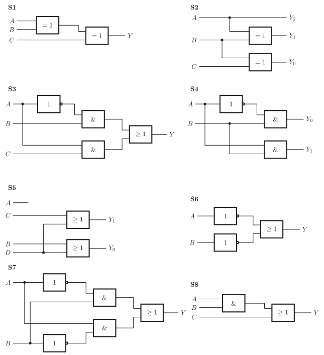
Schematics according to the standard of the International Electrotechnical Commission (IEC), IEC 60617:

VHDL code:
V1 – Inputs A, B, C; output Y:
Y <= (A or B) and C;V2 – Input X : bit_vector(1 downto 0); output Y : bit_vector(3 downto 0):
with X select
  Y <= "0001" when "00",
       "0010" when "01",
       "0100" when "10",
       "1000" when others;
V3 – Inputs A, B, C; outputs Y2, Y1, Y0:
Y2 <= A;
Y1 <= A xor B;
Y0 <= B xor C;
V4 – Input X : bit_vector(1 downto 0); output Y:
with X select
  Y <= '0' when "00",
       '1' when "01",
       '1' when "10",
       '0' when others;
V5 – Inputs A, B, C; output Y:
Y <= (A and B) or C;a) Assign each truth table T1 to T7 to the circuit in the list.
b) Assign each schematic S1 to S8 to the circuit in the list.
c) Assign each VHDL code V1 to V5 to the circuit in the list.
Solution
Given
Given explicitly:
- the list of the ten circuits
- the truth tables T1 to T7, the schematics S1 to S8 and the code V1 to V5 in the very high speed integrated circuit hardware description language (VHDL)
- each circuit appears in exactly two of the three forms
Known:
- Decoder and one-hot code (DET-05), encoder (DET-05), multiplexer (DET-05), demultiplexer (DET-05)
- Code converter from binary to Gray (DET-05), parity bit (DET-05, DET-05)
- NAND and XOR gates (DET-02, DET-02), De Morgan’s laws (DET-02)
- From the circuit to the expression (DET-02), from VHDL code to the circuit (DET-02), selected signal assignment (DET-05)
Required
a) to c) for each truth table, schematic and VHDL code its circuit
a) Truth tables
First count the inputs and outputs, then look for the pattern in the rows.
- T1: circuit 3, 2-to-1 multiplexer. Three inputs and one output. For , the output follows in the first four rows; for , it follows in the last four. So selects, and and are the data inputs: the 2-to-1 multiplexer (DET-05, 5.1).
- T2: circuit 6, parity generator with even parity for three data bits. Three inputs and one output, 1 for an odd number of ones. The output completes the three bits to an even number of ones: the parity generator with even parity (DET-05, 2.1).
- T3: circuit 1, 2-to-4 decoder. Two inputs and four outputs, and in each row exactly one output is 1, a one-hot code: the 2-to-4 decoder (DET-05, 3.1).
- T4: circuit 10, network that forms . Three inputs and one output, 1 only if and at least one of and is 1: the network that forms .
- T5: circuit 4, 1-to-2 demultiplexer. Two inputs and two outputs. For , both outputs are 0; for , the input reaches if and if . So selects, and is routed: the 1-to-2 demultiplexer (DET-05, 5.2).
- T6: circuit 2, 4-to-2 encoder. Four inputs, of which exactly one is 1 in each row, and two outputs that give the number of this input as a binary number, with as input 0 and as input 3: the 4-to-2 encoder (DET-05, 4.1).
- T7: circuit 7, NAND gate. Two inputs and one output, 0 only if both inputs are 1: the NAND gate (DET-02, 4.1).
Check for the tables with one output: each column agrees with the expression of its circuit in all rows.
The column of T7, under the expression of its circuit:
| 0 | 0 | 1 |
| 0 | 1 | 1 |
| 1 | 0 | 1 |
| 1 | 1 | 0 |
The columns of T1, T2 and T4, under the expressions of their circuits:
| 0 | 0 | 0 | 0 | 0 | 0 |
| 0 | 0 | 1 | 0 | 1 | 0 |
| 0 | 1 | 0 | 1 | 1 | 0 |
| 0 | 1 | 1 | 1 | 0 | 1 |
| 1 | 0 | 0 | 0 | 1 | 0 |
| 1 | 0 | 1 | 1 | 0 | 1 |
| 1 | 1 | 0 | 0 | 0 | 0 |
| 1 | 1 | 1 | 1 | 1 | 1 |
b) Schematics
Read each schematic from the inputs to the output, and write down the expression (DET-02, 6.1).
S1: circuit 6, parity generator with even parity for three data bits. Two XOR gates one behind the other, as the lesson builds a parity bit (DET-05, 4.3):
S2: circuit 5, code converter from binary to Gray with three bits. Three outputs: is , is and is : the code converter from binary to Gray (DET-05, 4.2).
S3: circuit 3, 2-to-1 multiplexer. An inverter, two AND gates and an OR gate: selects or , the 2-to-1 multiplexer (DET-05, 5.1):
S4: circuit 4, 1-to-2 demultiplexer. An inverter and two AND gates with two outputs: routes to or to , the 1-to-2 demultiplexer (DET-05, 5.2).
S5: circuit 2, 4-to-2 encoder. Two OR gates and an input that is not connected, as in the 4-to-2 encoder, whose input 0 is not needed (DET-05, 4.1): and .
S6: circuit 7, NAND gate. Two inverters and an OR gate. De Morgan’s law shows that this is the NAND operation (DET-02, 5.5):
S7: circuit 8, XOR gate. Two inverters, two AND gates and an OR gate: the output is 1 if the two inputs differ, the XOR operation (DET-02, 4.3):
S8: circuit 9, network that forms . An AND gate and an OR gate, in this order:
S6 shows that an operation can look quite different: the NAND gate as an OR gate with two inverted inputs.
c) VHDL code
Turn each operator into a gate (DET-02, 6.4), and read a selected signal assignment like a truth table.
- V1: circuit 10, network that forms . The parentheses give the OR operation first and then the AND operation: the network that forms .
- V2: circuit 1, 2-to-4 decoder. The selected signal assignment gives each code word of the input a pattern with exactly one 1: the 2-to-4 decoder (DET-05, 3.5).
- V3: circuit 5, code converter from binary to Gray with three bits. Three assignments, each a gate or a line: the code converter from binary to Gray (DET-05, 4.2).
- V4: circuit 8, XOR gate. The selected signal assignment delivers a 1 for the code words 01 and 10, where the two bits differ: the XOR operation (DET-05, 3.5, DET-02, 4.3).
- V5: circuit 9, network that forms . The parentheses give the AND operation first and then the OR operation: the network that forms .
Check: in a) to c) together, each of the ten circuits occurs exactly twice ✓