
Prof. Dr. Thorsten Jungmann (last updated 2026-11-02)
Relates to DET-05 Codes, code converters and standard components
Task
This list names ten circuits: six from this lesson, two derived gates and two small networks of basic gates.
- 2-to-4 decoder
- 4-to-2 encoder
- 2-to-1 multiplexer
- 1-to-2 demultiplexer
- code converter from binary to Gray with three bits
- parity generator with even parity for three data bits
- NAND gate
- XOR gate
- network that forms
- network that forms
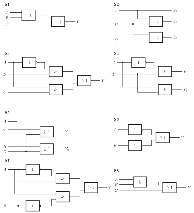
Below follow truth tables, schematics and code in the very high speed integrated circuit hardware description language (VHDL), whose inputs and outputs have neutral names. Each of the ten circuits appears in exactly two of the three forms.
Truth tables:
T1
| 0 | 0 | 0 | 0 |
| 0 | 0 | 1 | 0 |
| 0 | 1 | 0 | 1 |
| 0 | 1 | 1 | 1 |
| 1 | 0 | 0 | 0 |
| 1 | 0 | 1 | 1 |
| 1 | 1 | 0 | 0 |
| 1 | 1 | 1 | 1 |
T2
| 0 | 0 | 0 | 0 |
| 0 | 0 | 1 | 1 |
| 0 | 1 | 0 | 1 |
| 0 | 1 | 1 | 0 |
| 1 | 0 | 0 | 1 |
| 1 | 0 | 1 | 0 |
| 1 | 1 | 0 | 0 |
| 1 | 1 | 1 | 1 |
T3
| 0 | 0 | 0 | 0 | 0 | 1 |
| 0 | 1 | 0 | 0 | 1 | 0 |
| 1 | 0 | 0 | 1 | 0 | 0 |
| 1 | 1 | 1 | 0 | 0 | 0 |
T4
| 0 | 0 | 0 | 0 |
| 0 | 0 | 1 | 0 |
| 0 | 1 | 0 | 0 |
| 0 | 1 | 1 | 1 |
| 1 | 0 | 0 | 0 |
| 1 | 0 | 1 | 1 |
| 1 | 1 | 0 | 0 |
| 1 | 1 | 1 | 1 |
T5
| 0 | 0 | 0 | 0 |
| 0 | 1 | 1 | 0 |
| 1 | 0 | 0 | 0 |
| 1 | 1 | 0 | 1 |
T6
| 0 | 0 | 0 | 1 | 1 | 1 |
| 0 | 0 | 1 | 0 | 1 | 0 |
| 0 | 1 | 0 | 0 | 0 | 1 |
| 1 | 0 | 0 | 0 | 0 | 0 |
T7
| 0 | 0 | 1 |
| 0 | 1 | 1 |
| 1 | 0 | 1 |
| 1 | 1 | 0 |
Schematics according to the standard of the International Electrotechnical Commission (IEC), IEC 60617:

VHDL code:
V1 – Inputs A, B, C; output Y:
Y <= (A or B) and C;V2 – Input X : bit_vector(1 downto 0); output Y : bit_vector(3 downto 0):
with X select
  Y <= "0001" when "00",
       "0010" when "01",
       "0100" when "10",
       "1000" when others;
V3 – Inputs A, B, C; outputs Y2, Y1, Y0:
Y2 <= A;
Y1 <= A xor B;
Y0 <= B xor C;
V4 – Input X : bit_vector(1 downto 0); output Y:
with X select
  Y <= '0' when "00",
       '1' when "01",
       '1' when "10",
       '0' when others;
V5 – Inputs A, B, C; output Y:
Y <= (A and B) or C;a) Assign each truth table T1 to T7 to the circuit in the list.
b) Assign each schematic S1 to S8 to the circuit in the list.
c) Assign each VHDL code V1 to V5 to the circuit in the list.
Solution
a) T1: 3, T2: 6, T3: 1, T4: 10, T5: 4, T6: 2, T7: 7
b) S1: 6, S2: 5, S3: 3, S4: 4, S5: 2, S6: 7, S7: 8, S8: 9
c) V1: 10, V2: 1, V3: 5, V4: 8, V5: 9