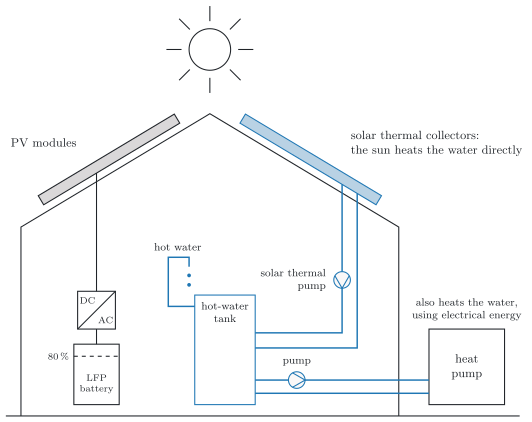
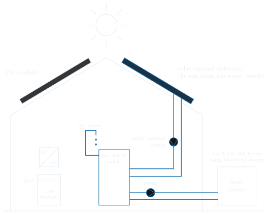
In our example system, an energy manager controls the heat pump through Smart Grid Ready (SG Ready). Its two switching signals A and B select one of four operating states: 0:0 is state 2, normal operation; 0:1 is state 3, boost; 1:0 is state 1, block; 1:1 is state 4, the start command. The energy manager selects state 3 when the photovoltaic (PV) system feeds surplus power into the grid; it never sends the start command, state 4. In states 1 and 2, the heat pump raises no set point. In state 3, it raises its set points for heating and for hot water, with two exceptions. In summer mode (German: Sommerbetrieb), the heating is off, and state 3 only raises the set point for hot water. While the solar thermal pump is running, the sun is already heating the hot water, and its set point is not raised. Besides A and B, the inputs and the outputs are:
C: summer mode is on
D: the solar thermal pump is running
Y: the set point for hot water is raised
Z: the set point for heating is raised
a) Set up the truth table of Y and Z. In the rows that never occur, mark the outputs as don’t cares.
b) Give Y and Z as minterm lists with don’t cares.
c) Minimize Y and Z with Karnaugh maps, using the don’t cares.
d) Describe the minimized circuit in VHDL.
e) What do your minimized circuits deliver if the energy manager sends the start command after all?
the SG Ready signals A and B: 0:0 state 2, normal operation; 0:1 state 3, boost; 1:0 state 1, block; 1:1 state 4, start command
the inputs C (‘summer mode on’) and D (‘solar thermal pump running’)
the outputs Y (‘set point for hot water raised’) and Z (‘set point for heating raised’)
the rule: states 1 and 2 raise no set point; state 3 raises both set points, in summer mode only the one for hot water, and while the solar thermal pump is running not the one for hot water; the start command never occurs
Known:
SG Ready: two signals, four operating states (DET-02)
Don’t cares in the truth table, in the minterm list and in the Karnaugh map (DET-03)
The Karnaugh map with four inputs and loops of ones (DET-03, DET-03)
a) the truth table of Y and Z with don’t cares
b) the minterm lists of Y and Z with don’t cares
c) the minimized expressions of Y and Z
d) the VHDL code of the minimized circuit
e) the outputs of the minimized circuits for the start command
a) Truth table
Only state 3, with A=0 and B=1, raises a set point; in states 1 and 2, both outputs are 0 (DET-02, 6.6). State 3 covers rows 4 to 7:
The set point for hot water is raised unless the solar thermal pump is running: Y is 1 in rows 4 and 6, where D is 0.
The set point for heating is raised unless summer mode is on: Z is 1 in rows 4 and 5, where C is 0.
The energy manager never sends state 4, with A=1 and B=1. Rows 12 to 15 therefore never occur, and their outputs are don’t cares, marked X (DET-03, 4.4):
Row
A
B
C
D
Y
Z
0
0
0
0
0
0
0
1
0
0
0
1
0
0
2
0
0
1
0
0
0
3
0
0
1
1
0
0
4
0
1
0
0
1
1
5
0
1
0
1
0
1
6
0
1
1
0
1
0
7
0
1
1
1
0
0
8
1
0
0
0
0
0
9
1
0
0
1
0
0
10
1
0
1
0
0
0
11
1
0
1
1
0
0
12
1
1
0
0
X
X
13
1
1
0
1
X
X
14
1
1
1
0
X
X
15
1
1
1
1
X
X
Check with two rows of state 3: in row 4, without summer mode and without sun, both set points are raised; in row 7, in summer mode and with sun, neither is ✓
b) Minterm lists with don’t cares
The minterm list names the rows with a 1; after it, d names the don’t cares (DET-03, 4.4):
Check: both lists contain a 1 only in rows of state 3, rows 4 to 7, and the four rows of state 4 as don’t cares ✓
c) Minimization with don’t cares
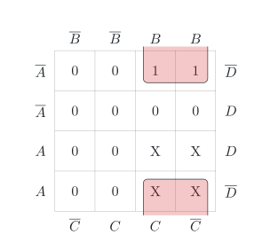
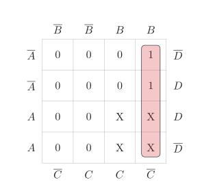
In the Karnaugh map with four inputs, A stands on the left of the rows and D on the right of them, B above and C below the columns. Row by row, the cells contain the minterms 0, 2, 6 and 4; 1, 3, 7 and 5; 9, 11, 15 and 13; 8, 10, 14 and 12 (DET-03, 4.1). The don’t cares of state 4, in the cells of 12 to 15, form a square at the bottom right. When you draw the loops, each X may count as a 1 or as a 0, whichever gives larger loops (DET-03, 4.4).
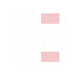
For Y, the ones in the cells of 4 and 6 lie in the top row, in the two right columns (figure). Without don’t cares, they would form a loop of two only, A⋅B⋅D. With the X in the cells of 12 and 14 at the bottom of the same columns, the loop grows across the top and the bottom edge to four cells. In all four, B is 1 and D is 0, while A and C change (DET-03, 4.2):
Y=B⋅D
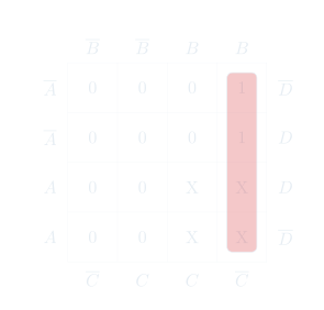
For Z, the ones in the cells of 4 and 5 lie in the last column, in the two upper rows (figure). With the X in the cells of 13 and 12 below them, the whole last column becomes a loop of four. In all four cells, B is 1 and C is 0, while A and D change:
Z=B⋅C
The don’t cares have removed A from both terms: the minimized circuits do not need the signal A at all. The X that lie in no loop, in the cells of 13 and 15 for Y and of 14 and 15 for Z, count as 0.
Check: B⋅D is 1 in rows 4, 6, 12 and 14, that is, in the two rows with a 1 of Y and in two of its don’t cares; B⋅C is 1 in rows 4, 5, 12 and 13, the two rows with a 1 of Z and two of its don’t cares ✓
d) VHDL
Step 5 describes the minimized circuit in VHDL, as in the lesson (DET-03, 6.3). Each expression becomes a signal assignment; each not becomes an inverter, each and an AND gate with two inputs:
-- A, B: SG Ready signals, C: summer mode-- D: solar thermal pump running-- Y: set point for hot water raised-- Z: set point for heating raisedentity boost is port (A, B, C, D : in bit; Y, Z : out bit);end entity;architecture behaviour of boost isbegin Y <= B and not D; Z <= B and not C;end architecture;
The entity describes the interface of the circuit with all four signals, also A, which the minimized circuit does not use. The two assignments are concurrent, so their order does not matter.
Check in row 4, with A=0, B=1, C=0 and D=0, where both set points are raised:
B⋅DB⋅C=1⋅0=1=1⋅0=1
Both assignments deliver a 1, as row 4 of the truth table demands ✓
e) The start command
State 4 means A=1 and B=1. The minimized expressions no longer contain A. For A=1 and B=1:
YZ=B⋅D=1⋅D=D=B⋅C=1⋅C=C
The circuits treat the start command like state 3: they raise the set point for hot water unless the solar thermal pump is running, and the set point for heating unless summer mode is on. This follows from the loops of c), which counted the don’t cares in the cells of 12 and 14 for Y and of 12 and 13 for Z as ones. A finished circuit always delivers a definite value, also for a combination that was a don’t care (DET-03, 4.4). Since the energy manager never sends the start command, this does no harm; if the combination occurred after all, because of a fault or a later change, the heat pump would react with these values.
Check in row 14, with C=1 and D=0: for Y, D=0=1, and for Z, C=1=0. In the maps of c), the cell of 14 lies in the loop of Y and outside the loop of Z ✓
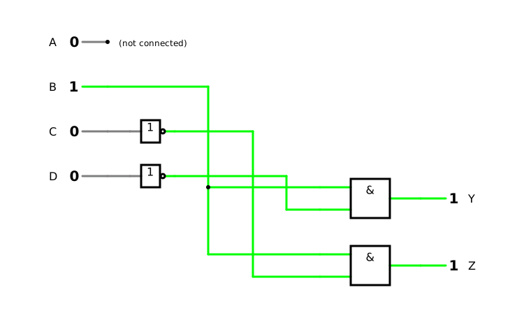
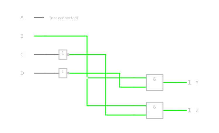
The simulation shows the minimized circuit. It starts in state 3, without summer mode and without sun: both outputs show 1. Switch C and D to see the two exceptions. The input A is not connected: if you also switch it to 1, the inputs stand for the start command, and the outputs do not change. The circuit treats the start command like state 3, as e) shows.